Imageamento por MEV de Amostras Biológicas
English
分享
概述
Fonte: Peiman Shahbeigi-Roodposhti e Sina Shahbazmohamadi, Departamento de Engenharia Biomédica, Universidade de Connecticut, Storrs, Connecticut
Um microscópio eletrônico de varredura (SEM) é um instrumento que usa um feixe de elétrons para imagem não destrutiva e caracterizar materiais condutivos em um vácuo. Como analogia, um feixe de elétrons é para o SEM como a luz é para o microscópio óptico. A diferença é que o microscópio eletrônico produz imagens de resolução e ampliação muito maiores. Os melhores microscópios ópticos normalmente têm uma resolução de até 200 nm, enquanto os SEMs geralmente reivindicam uma resolução de 0,5 nm. Isso se deve ao fato de que os microscópios ópticos são limitados pela difração das ondas, uma função do comprimento de onda, que é em torno de 500 nm para luz visível. Por outro lado, o SEM usa um feixe de elétrons energizado, que como um comprimento de onda de 1 nm. Essa característica as torna ferramentas muito confiáveis para o estudo de nano e microestruturas. Microscópios eletrônicos também permitem o estudo de amostras biológicas com tamanhos de características muito pequenos para microscopia óptica.
Esta demonstração fornece uma introdução à preparação da amostra e aquisição inicial de imagens de amostras biológicas usando um microscópio eletrônico de varredura. Neste caso, será estudado um andaime celular de colágeno-hidroxiapatita (HA). O ambiente de vácuo do SEM e o carregamento induzido pelo feixe de elétrons em amostras não condutoras (como matéria orgânica) criam desafios que serão abordados na preparação. As vantagens e desvantagens de diferentes métodos de imagem no que se referem à resolução, profundidade de foco e tipo de amostra também serão discutidas. O objetivo desta demonstração é dar ao participante mais informações sobre o SEM para determinar se este módulo de microscopia é o melhor adequado para um tipo de amostra biológica.
Principles
Procedure
Results
The SEM images in Figures 3 and 4 show that the imaged structure is highly three dimensional with microscale features. Image quality is affected by the focus and the thickness of the sputter coating.
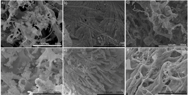
Figure 3: The following images demonstrate how the sample focus can affect image quality. In the image on the right, the whole field of view is in focus, whereas it is out of focus on the left. Playing with parameters like the focus can provide a much better image.

Figure 4: Images of collagen-hydroxyapatite sample.
Applications and Summary
Here we demonstrated the depth of focus, field of view and maximum resolution and magnification of an electron microscope and how these properties can be used to view biological samples. This demonstration was designed to help viewers decide which microscopy module is the best for a certain application. As demonstrated, SEM has a very high depth of focus, much higher resolution and greater magnifications. However, it is not appropriate for all sample types.
This demonstration introduced the principles of electron microscopy and showed several of their applications in research labs. Electron microscopes are used for inspection, characterization and quality control. For example, they are used to visualize ICs, circuit boards, crack propagation and nano-electromechanical systems. In the field of biology these instruments play a key role as well. There are even electron microscopes especially designed to accommodate wet biological samples. These biological samples range from tissues to bone, cells and microorganisms. Using additional detectors can enable even more analysis, such as precise surface analysis.
Materials List
| Name | Company | Catalog Number | Comments |
| Equipment | |||
| Biosample | |||
| Carbon or Gold coater | |||
| Cross beam-SEM | ZEISS | ||
| Collagen-Hydroxyappetite Cellular Scaffolds | Developed by Wei Laboratory at University of Connecticut |
References
- Oatley, C. W., W. C. Nixon, and R. F. W. Pease. "Scanning electron microscopy." Advances in Electronics and Electron Physics 21 (1966): 181-247.
- Goldstein, Joseph, et al. Scanning electron microscopy and X-ray microanalysis: a text for biologists, materials scientists, and geologists. Springer Science & Business Media, 2012.
- Carol Heckman, et al. Preparation of cultural cells for scanning electron microscope. Nature Protocols Network, 2007, doi:10.1038/nprot.2007.504
成績單
Scanning electron microscopy, or SEM, is often used to image biological materials on the nano scale. Optical microscopes, which use light to image a sample, are heavily used to non-destructively image biological samples, however, their resolution and depth of field is limited, thus SEM is used in order to achieve higher resolution down to one nanometer.
In SEM, a beam of electrons is focused through a series of condenser lenses, which then hits the sample. When the beam hits the sample, electrons on the surface are scattered and measured by the detector.
In this video, we will discuss how SEM works, demonstrate how to image a biological sample in the laboratory, and finally, introduce some techniques used to image sensitive samples.
A scanning electron microscope uses a high energy electron beam, which is generated by an electron gun fitted with a filament cathode. The generated electrons are propelled toward the anode and then focused using condenser lenses before entering the objective lens. The objective lens is calibrated to focus the beam on the sample, where it is raster scanned across the surface. The interactions of the electrons with the atoms in the sample are used to study the topography, elemental composition, and crystallinity of the sample. When the incident electron beam hits the surface, it emits secondary and backscattered electrons. Secondary electrons are low energy electrons that are emitted from the sample close to the surface and provide topographical information.
Backscattered electrons, on the other hand, are reflected in the opposite direction of the incident beam. The interaction intensity increases with increasing atomic weight, enabling the user to distinguish compositional differences. Special consideration is needed to image biological samples with SEM, since SEM utilizes a high vacuum, thus biological samples, which typically have a high water content, must be dried first. This can cause collapse of the structure of sensitive samples, especially cells. Thus, cells are treated with a fixative, rinsed, and then dehydrated slowly by washing with increasing amounts of ethanol.
For rigid biological materials, such as the collagen-hydroxyapatite tissue scaffold used in this demonstration, the sample is dried over a period of several days under high vacuum.
Finally, since typical SEM imaging requires a conductive surface, biological samples are often sputter coated with a thin layer of metal prior to imaging. Now that we’ve discussed how SEM works and how to prepare a biological sample for imaging, let’s take a look at how to prepare and image a collagen-hydroxyapatite tissue scaffold.
First, mount the biomaterial sample onto an SEM stub using conductive carbon tape and ensure that the sample is dry and has no contamination on the surface.
Then, place the mounted sample in the chamber of a sputter coater, pump down the chamber, and sputter coat the sample for around 40 seconds to achieve a thin, four- to six-nanometer thick coating of metal, in this case gold, with adequate coverage. Once coated, remove the sample and use conductive tape to connect the stub to the top of the sample, which is now coated with conductive metal.
Finally, mount the stub on the SEM stage and tighten the screw on the side. Now the sample is ready to image with SEM. First, load the stage into the SEM chamber and seal the door, then hit the transfer button to open the passage from the loading chamber to the vacuum. Once the internal door is open, screw the metal rod into the stage and push the sample into the vacuum chamber, then unscrew the metal rod and fully retract it into the load chamber, then press store to close the vacuum chamber.
Now let’s image the sample using SEM.
First, move the stage using the controller and navigate the sample into the field of view, then move the sample vertically until the working distance is five to 10 millimeters. Turn the electron beam on and select the detector for secondary electrons, set the beam to five kiloelectron volts initially, then increase up to 20 to 30 kiloelectron volts as needed. If the image is not clear, turn the focus, brightness, and contrast knobs until a clear image appears.
Use the stage navigation and the X and Y directions to locate a new spot on the sample, then increase the magnification until the desired features are visible. Adjust the focus, contrast, and brightness as needed to improve the image quality. You may need to decrease the scan speed and turn on line averaging to acquire a better image, then save the image.
The SEM images reveal a highly three-dimensional and porous structure with fibrous features smaller than 25 microns. These features would be difficult to visualize using optical microscopy, as optical microscopy has a much lower depth of field.
There are many challenges associated with the imaging of biological structures with SEM, including structure collapse or damage from the high energy electron beam. Let’s now take a look at how the general SEM technique is applied to these types of sensitive samples. Delicate biological structures, such as these young plant tissues, or those with a high water content, must be treated through a fixation process prior to imaging.
These floral meristems were immediately treated with a freshly prepared formalin/acetic acid fixative solution. The fixed tissue was dissected in ethanol, placed in a mesh container, and dehydrated through an ethanol series of 70%, 80%, 90%, and 100% ethanol. Finally, the plant tissues were dried using a critical point dryer, mounted, and sputter coated with a thin metal coating.
After SEM imaging, it is clear that the untreated structures were heavily damaged by the drying process and showed considerable collapse in structure, while those that were fixed maintained their native structure. Alternatively, cells and other high water content specimens can be imaged using environmental SEM, or ESEM. ESEM utilizes a high energy electron beam that is raster scanned over the sample, as with conventional SEM, however, it enables the imaging of wet or uncoated samples by maintaining a gaseous environment within the chamber.
This is done by separating the high vacuum chamber containing the electron gun from the specimen chamber using two apertures. The electron beam does incur significant losses due to scattering by gas molecules, but is typically a high enough energy for imaging. Here, cells were grown on a silicon chip, functionalized with quantum dots, and fixed using a glutaraldehyde fixation protocol. The cells were imaged in water and show the uncollapsed structure of the cell with individual quantum dots visible on the cell surface.
You’ve just watched JoVE’s introduction to visualizing biomaterials using SEM. You should now understand how SEM works, how biological samples are prepared and imaged, as well as some applications of the technique for sensitive structures.
Thanks for watching!