We describe the device fabrication and measurement protocol for carbon nanotube based high frequency biosensors. The high frequency sensing technique mitigates the fundamental ionic (Debye) screening effect and allows nanotube biosensor to be operated in high ionic strength solutions where conventional electronic biosensors fail. Our technology provides a unique platform for point-of-care (POC) electronic biosensors operating in physiologically relevant conditions.
The unique electronic properties and high surface-to-volume ratios of single-walled carbon nanotubes (SWNT) and semiconductor nanowires (NW) 1-4 make them good candidates for high sensitivity biosensors. When a charged molecule binds to such a sensor surface, it alters the carrier density5 in the sensor, resulting in changes in its DC conductance. However, in an ionic solution a charged surface also attracts counter-ions from the solution, forming an electrical double layer (EDL). This EDL effectively screens off the charge, and in physiologically relevant conditions ~100 millimolar (mM), the characteristic charge screening length (Debye length) is less than a nanometer (nm). Thus, in high ionic strength solutions, charge based (DC) detection is fundamentally impeded6-8.
We overcome charge screening effects by detecting molecular dipoles rather than charges at high frequency, by operating carbon nanotube field effect transistors as high frequency mixers9-11. At high frequencies, the AC drive force can no longer overcome the solution drag and the ions in solution do not have sufficient time to form the EDL. Further, frequency mixing technique allows us to operate at frequencies high enough to overcome ionic screening, and yet detect the sensing signals at lower frequencies11-12. Also, the high transconductance of SWNT transistors provides an internal gain for the sensing signal, which obviates the need for external signal amplifier.
Here, we describe the protocol to (a) fabricate SWNT transistors, (b) functionalize biomolecules to the nanotube13, (c) design and stamp a poly-dimethylsiloxane (PDMS) micro-fluidic chamber14 onto the device, and (d) carry out high frequency sensing in different ionic strength solutions11.
When a charged molecule binds to a SWNT or NW electronic sensor, it can either donate/accept electrons or act as a local electrostatic gate. In either case, the bound molecule can alter the charge density in the SWNT or NW channel, leading to a change in the measured DC conductance of the sensor. A large variety of molecules15-20 have been successfully detected by studying DC characteristics of the nanosensors during such binding events. Even though charge-detection based sensing mechanism has many advantages including label-free detection21, femto-molar sensitivity22, and electronic read out capability15; it is effective only in low ionic strength solutions. In high ionic strength solutions, DC detection is impeded by ionic screening6-8. A charged surface attracts counter-ions from the solution which forms an electrical double layer (EDL) near the surface. The EDL effectively screens off these charges. As the ionic strength of the solution increases, the EDL becomes narrower and the screening increases. This screening effect is characterized by the Debye screening length λD,
, where ε is the dielectric permittivity of the media, kB is the Boltzmann’s constant, T is the temperature, q is the electron charge, and c is the ionic strength of the electrolyte solution. For a typical 100 mM buffer solution, λD is around 1 nm and the surface potential will be completely screened at a distance of a few nm. As the result, most of nanoelectronic sensors based on SWNTs or NWs operate either in dry state20 or in low ionic strength solutions5,15,17,21-22 (c ~ 1 nM – 10 mM); otherwise the sample needs to undergo desalting steps15,23. Point-of-care diagnostic devices need to operate in physiologically relevant ionic strengths at patient site with limited sample processing capability. Hence, mitigating ionic screening effect is critical for development and implementation of POC nanoelectronic biosensors.
We mitigate the ionic screening effect by operating SWNT based nanoelectronic sensor at megahertz frequency range. The protocol provided here details the fabrication of a SWNT transistor based nanoelectronic sensing platform and high frequency mixing measurement for biomolecular detection. The single-walled carbon nanotubes are grown by chemical vapor deposition on substrates patterned with Fe catalysts24. For our SWNT transistors, we incorporate a suspended top-gate25 placed 500 nm above the nanotube, which helps enhance high frequency sensor response and also allows for a compact micro-fluidic chamber to seal the device. The SWNT transistors are operated as high frequency mixers9-11 in order to overcome the background ionic screening effects. At high frequencies, the mobile ions in solution do not have sufficient time to form the EDL and the fluctuating biomolecular dipoles can still gate the SWNT to generate a mixing current, which is our sensing signal. The frequency mixing arises due to the nonlinear I-V characteristics of a nanotube FET. Our detection technique differs from the conventional techniques of charge based detection and impedance spectroscopy26-27. Firstly, we detect biomolecular dipoles at high frequency rather than the associated charges. Secondly, the high transconductance of SWNT transistor provides an internal gain for the sensing signal. This obviates the need for external amplification as in case of high frequency impedance measurements. Recently, other groups have also addressed biomolecular detection in high background concentrations23,28. However, these methods are more involved, requiring complex fabrication or careful chemical engineering of receptor molecules. Our high frequency SWNT sensor incorporates a simpler design and utilizes the inherent frequency mixing property of a nanotube transistor. We are able to mitigate the ionic screening effects, thus promising a new biosensing platform for real-time point-of-care detection, where biosensors functioning directly in physiologically relevant condition are desired.
1. Catalyst Patterning for SWNT Growth
Tip: Design pits of different sizes e.g. 5 micron x 5 micron, 10 micron x 5 micron etc. to account for the variability in SWNT chemical vapor deposition (CVD) growth process.
2. CVD Growth of Carbon Nanotubes
Tip: Determine sweet spot for nanotube growth. Growth is uniform over an area of 2inch x 2inch downstream for our furnace (Figure 2c).
3. SWNT FET Transistor Fabrication
Tip: Extend electrode contact pads far apart on the die so that they remain accessible even after putting down a micro-fluidic stamp on the active nanotube region.
Tip: Use thick chrome layer to increase strength of suspended top gate. Gate dimensions are also critical for successful suspension.
Tip: Etch time calibration is recommended.
4. Chemical Functionalization of Carbon Nanotube Sidewalls
Note: We rinse the die by dispensing DI water (~50 ml) over the die using a squeeze bottle. Then we move the die to another Petri dish containing DI water and move the die around for 1 min. We repeat the two steps a total of 8-10 times.
5. Preparation of Polydimethylsiloxane (PDMS) Mold for Fluid Chamber
Tip: If the mixture starts foaming, vent the chamber and let it settle down for a few seconds before degassing again.
Tip: The PDMS side directly in contact with the silicon wafer is clean and extremely flat. This side will be in contact with the SWNT FET die. Be careful not to contaminate it.
Tip: This can be done with the naked eye or using an optical microscope with enough working space. If the PDMS does not stick well (generally if the die and/or the PDMS stamp is not clean), do oxygen plasma (20 watts, 15 sec) on PDMS to assist bonding. Using plasma powers higher than this leads to stronger bonding, however, we have seen ripping of electrodes while removing the PDMS in such case.
6. Preparation of Microfluidic Flow Channel
Tip: To avoid collapse of structure a channel width: height ratio of 10:1 is sufficient (300 μm: 30 μm in this case).
7. DC Electrical Measurement Setup
Tip: For measurements in solution, keep gate voltage sweep parameter within |0.7 volts| to avoid leakage and reaction between the gate metal electrode and solution.
8. AC Electrical Measurement Setup
9. Electrical Measurements in Solution (No Flow)
Tip: Use pipette to withdraw previous solution and then flush the chamber multiple times with the new solution. Always switch from the low to high concentration solutions.
10. Electrical Measurement in Solution (Real Time Flow)
A scanning electron microscope image of SWNT transistor with a suspended top gate is shown in Figure 7a. The gate dimensions are critical for suspension25. The current design dimensions are (length x width x thickness = 25 μm x 1 μm x 100 nm). The gate electrode consists of 50 nm Cr/50 nm Au; a thick chrome layer adds more strength to suspended structure. The suspended structure is confirmed by absence of leakage current between top gate and drain (Figure 7b).
We use the biotin-streptavidin ligand-receptor system to evaluate our SWNT sensor. To characterize the success of sidewall functionalization we monitor the FET DC transfer curves in air after each functionalization step. Figure 7c illustrate that the transfer curve shift to the right after biotinylation (red) and streptavidin binding (blue). This can be attributed to the electrostatic gating by the electronegative amine groups present on biotin PEO-amine and streptavidin.
For high frequency measurements, we follow the schematic shown in Figure 5b. The non linear I-V characteristics of SWNT transistor, mixes the high frequency inputs at the source and gate to yield a mixing current output, Imix which is our sensing signal. Figure 7d shows Imix measured as a function of gate voltage for a typical device in 100 mM NaCl. The mixing current for an AM modulated input at modulation frequency, ωm, is given by10-11
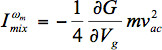
, where m is the modulation depth, vac is the AM input amplitude and ∂G/∂Vg is the transconductance of the device (slope of the Idc-Vg curve in Figure 7d). The mixing current results (m = 0.78 and vac = 20mV) agree well with the model as shown in the figure. For static fluidic measurements, we compare the peak of such mixing current sweeps for functionalized nanotubes. For flow measurements, we fix carrier frequency of AM modulated signal and fix gate voltage (Vg = 0) and monitor Imix for biomolecular binding as a function of time, while maintaining a steady fluid flow. Figure 7e-7f shows the representative results for both static and flow measurements respectively.
For biomolecular detection, it is necessary that the CNT is exposed directly to the solution i.e. SiO2 is completely etched away during the BHF etch step. If this condition is not met, the chemical modification of CNT’s is not possible as the linker molecule cannot stack along the nanotube sidewall. This is clearly illustrated in Figure 7g where we see no change before and after binding even in DI water for a SiO2 passivated device. This also proves that our measurement results indicate successful chemical modification as well as biomolecular detection in high background ionic concentrations. In all the measurements, we observe that the sensor response drops beyond 30 MHz which is due to resonance from setup.
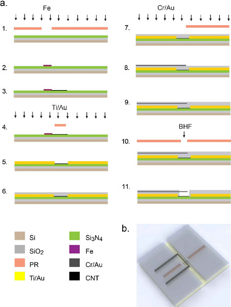
Figure 1. Nanotube transistor fabrication process flow. (a) Fabrication process – (1) Photomask layer-1 (PL-1) for catalyst deposition, (2) metal liftoff, (3) CNT growth, (4) PL-2 for source-drain contact, (5) metal liftoff, (6) SiO2 blanket deposition, (7) PL-3 for gate contact, (8) metal liftoff, (9) Thin SiO2 blanket deposition, (10) PL-4 for BHF wet etch channel and (11) final device after photoresist removal. Color scheme is illustrated. (b) Schematic of device structure.
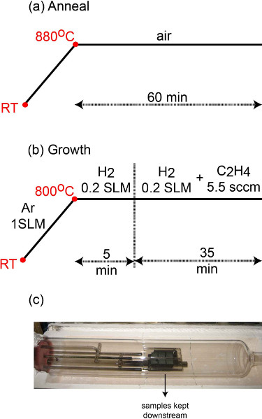
Figure 2. Carbon Nanotube growth. (a) Anneal step to remove photoresist residue, (b) growth step for CNT growth and (c) device placement in growth furnace.
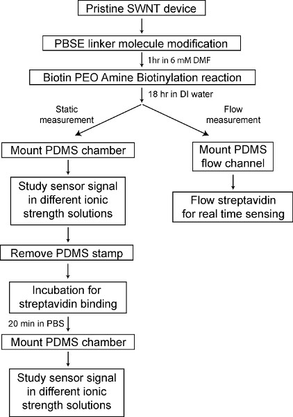
Figure 3. Flowchart for chemical functionalization of CNT.
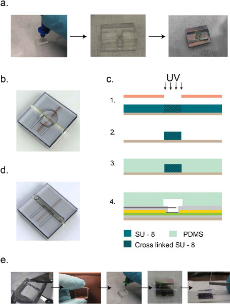
Figure 4. PDMS stamp for solution measurements. (a)-(b) Static (no flow) measurements. (a) Punching and mounting a PMDS chamber on device, (b) Schematic diagram of flow chamber on a device. (c)-(e) Flow measurements. (c) Process flow for PDMS flow channel using SU-8 mold. (1) Photomask for defining flow channel, (2) cross linked SU-8 mold, (3) PDMS on SU-8 and (4) PDMS flow channel stamped onto device. (d) Schematic diagram of flow channel on a device and (e) Punching inlet/outlet holes in PDMS, stamping the flow channel on device and connecting polyethylene tubing to inlet/outlet ports.
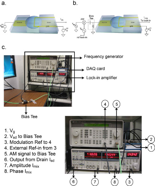
Figure 5. Electrical measurement setup. (a) DC measurement schematic, (b) AC mixing current measurement schematic and (c) image of experimental setup for AM modulated frequency mixing measurement. Click here to view larger figure.
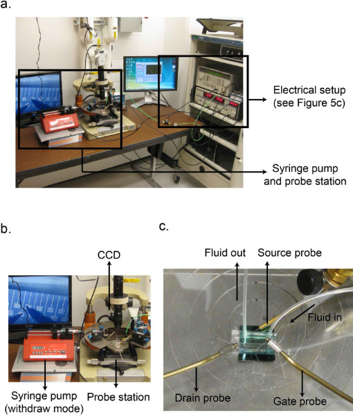
Figure 6. Flow measurement setup. (a) Image of entire measurement setup; (b) Syringe pump and probe station; and (c) image of device with PDMS flow channel, inlet/outlet flow tubes and electrical probes.
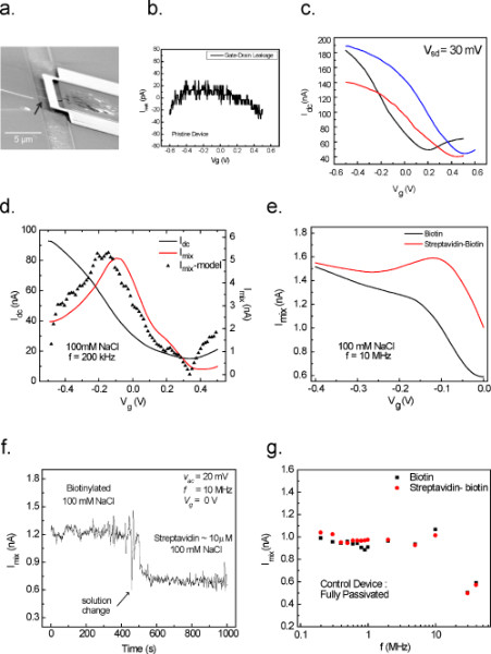
Figure 7. Representative results for SWNT biosensor. (a) SEM image of a typical suspended top-gate device, (b) gate-drain leakage to confirm suspended structure, (c) Idc-Vg curve for pristine nanotube FET (black), after biotinylation (red) and after streptavidin binding (blue) measured in air, (d) DC current, Idc (black, Vsd = 10 mV) and mixing current, Imix (red, modulation f = 200 kHz) as a function of Vg for the device in 100 mM NaCl solution. Theoretical Imix obtained using the model in equation (1) is also shown (▲) for comparison. (e) Imix-Vg curves for biotinylated (black) and streptavidin-biotin bound (red) SWNT in 100 mM NaCl at f = 10 MHz, (f) real time flow measurement to detect streptavidin binding in 100 mM NaCl and (g) signal change after binding in a fully passivated control device in DI water at different frequencies. Click here to view larger figure.
The growth of carbon nanotubes depends not only on furnace conditions but also substrate cleanliness. The optimal gas flow rate, temperature and pressure for growth have to carefully calibrated and once fixed they are more or less stable. Even with these conditions being met, we found that growth depends on the patterned catalyst area, amount of catalyst and substrate cleanliness. Hence, we incorporated multiple catalyst pit sizes to account for the variability in growth. A one hour high temperature anneal step helped remove any contaminants like PR residue etc. from the substrate. Figure 2 illustrates the conditions we adopted for SWNT growth.
The presence of contaminants from die processing steps may lead to spurious signal in chemical and biological sensing. Hence, it is necessary to clean the substrate thoroughly before and after chemical functionalization. The rinsing steps after each functionalization helps remove any excess reagent which may adhere to the device near the active area. We also observed that if the substrate was not clean, the PDMS stamp was not leak-tight and peeled off with fluid pressure during measurements. In such cases, very gentle O2 plasma on PDMS stamp helped adhesion. Too strong an O2 plasma may make the PDMS stamp stick well but hard to remove from the device; we have noticed ripping of electrodes while removal which renders the die unusable. If the PDMS stamp and the die are clean, the adhesion between them is good enough to survive fluid flow measurements without oxygen plasma treatment also. Do not use O2 plasma on the SWNT device as this will etch the carbon nanotubes.
In solution based electrical measurements, any leakage current overwhelms the detection signal. This leakage happens because the solution too can act as a conductor, the resistance of which goes down with increasing salt concentration. Therefore, it is necessary to incorporate electrode passivation step in the transistor design. The two blanket depositions in our fabrication protocol (500 nm and 20 nm SiO2) helped reduce leakage from source, drain and gate metal contacts. Also, before taking any electrical measurement, a gate-drain leakage sweep is recommended to ensure that no leakage happens in the intended sweep voltage range.
For fluid flow measurements, it is necessary to avoid air traps in the flow channel. The air gap leads to signal distortions because the sensor response in air is different than when in solution. In the forward pumping mode this issue was often encountered which impeded fluid flow. This was avoided by operating the syringe pump in withdrawal mode.
For the high frequency electrical measurements in high background ionic solutions the response dropped beyond 30-40 MHz due to the resonance loss from the measurement setup. We believe this can be improved by designing devices with lower parasitics. Optimized gate-SWNT distance and smaller BNC and SMA cables may help improve sensitivity.
The authors have nothing to disclose.
We thank Prof. Paul McEuen at Cornell University for early discussion. The work is supported by the start-up fund provide by the University of Michigan and the National Science Foundation Scalable Nanomanufacturing Program (DMR-1120187). This work used the Lurie Nanofabrication Facility at University of Michigan, a member of the National Nanotechnology Infrastructure Network funded by the National Science Foundation.
REAGENTS | |||
Reagents which were provided within Lurie Nanofabrication Facility (University of Michigan) are marked as LNF in the catalogue column. Chemicals which require protective equipment (gloves, safety goggles, face mask, apron) and/or fume hood are denoted with PPE in comments section. | |||
Silicon wafers (P-type, <100>, 500-550 μm thick) | Silicon Valley Microelectronics | ||
SPR 220 3.0 | Dow (Rohm and Haas) | Megaposit SPR | PPE |
AZ 300MIF | AZ Electronic Material Corporation | PPE | |
Acetone | J T Baker | 9005-05 | PPE |
Isopropanol (IPA) | J T Baker | 9079-05 | |
Buffered Hydrofluoric Acid | Transene | PPE | |
1-Pyrene Butanoic Acid, succinimidyl ester | Molecular Probes | P130 | PPE |
Biotin PEO Amine | Thermo Scientific | EZ- Link PEG2 Biotin, # 21346 | PPE |
Streptavidin | Invitrogen | S 888 | PPE |
Dimethylformamide | MP Biomedicals | 0219514791 | PPE |
Polydimethylsiloxane Elastomer Base and Curing Agent | Dow Corning | Sylgard 184 Elastomer Kit | PPE |
SU-8 2015 | Microchem | Y111064 | PPE |
SU-8 Developer | Microchem | Y020100 | PPE |
Silanizing agent | Sigma Aldrich | 452807 | PPE |
Hydrogen | Purity Plus | LNF | |
Ethylene | Purity Plus | LNF | |
Argon | Purity Plus | LNF | |
Phosphate Buffer Saline System | Sigma Aldrich | PBS1 | |
EQUIPMENT | |||
Equipment provided by Lurie Nanofabrication Facility (University of Michigan) is denoted as LNF in Catalogue column. | |||
GCA 200 Autostepper | GCA | LNF | |
Low Pressure Chemical Vapor Deposition Tool | Tempress | LNF | |
e-beam Evaporator | Enerjet | LNF | |
CNT growth Furnace | First Nano | Easy Tube 3000 (LNF) | |
Photomasks | Nanofilm | LNF | |
Petri dish (150mm) | LNF | ||
Desiccator | Bel-Art | F420100000 | |
Biopsy Punch | Ted Pella | 15071/78 | |
Scalpel | Ted Pella | 548 | |
Polyethylene Tubing PE-50 | VWR | 20903-414 | |
Syringe Pump | New Era Pump Systems | NE-1000 | |
Syringe | Fisher Scientific | BD Safety-Lok Syringes | |
Syringe Needles | Fisher Scientific | 14-821-13A | |
DAQ card | National Instruments | 779111-01 | |
GPIB connector | National Instruments | 778032-51 | |
Lock-in Amplifier | Stanford Research Systems | SR 830 | |
Frequency Generator | HP Agilent | 8648B, 9kHz -2GHz | |
Bias Tee | Picosecond | 5575A-104 | |
Current Preamplifier | DL Instruments, LLC | DL 1211 | |
BNC cables | Allied Electronics | 665-xxxx | |
SMA cables | Sentro Tech Corp | SCF65141 |