Neuroprosthetic devices aim to restore impaired or absent sensory and motor abilities in a wide range of patient populations, including those with spinal cord injury, Amyotrophic Lateral Sclerosis (ALS), cerebral palsy, and amputations1,2,3. Intracortical microelectrodes (IMEs) can establish a communication pathway between cortical neurons and the devices used to control neuroprosthetics. A distinct advantage of intracortical microelectrodes is their capability to record neural signals at the high spatial and temporal resolution, which is preferred for subsequent signal processing and control of brain-computer interfaces4,5. Unfortunately, the performance of intracortical microelectrodes dramatically reduces within months to a year following implantation2,6,7,8. The loss of signal quality and stability negatively affects the application of the technology.
A significant contributor to the observed performance decline is the biotic response to implantation-associated tissue damage and chronic neuroinflammation9,10,11. Implantation of IMEs inflicts damage on brain tissue, resulting in the release of signaling molecules that initiate cascades of reactionary cellular defense processes. Chronic interfacing exacerbates the foreign body response, leading to sustained neuroinflammation that damages tissue proximal to the device; often recognized as symptoms of neuroinflammation, scarring, and local neurodegeneration contributing to the decline of the recording of the signal quality12,13,14,15. Comprising a dense conglomerate of astrocytes with entrained activated microglia and macrophages, the scar that encapsulates the electrode creates an unfavorable local environment with reduced material transport and local accumulation of inflammatory factors16,15,16,17,18.
Many studies have described the brain's response to intracortical microelectrodes or approaches to mitigate the response7. Research and development into improving the tissue response have involved a range of strategies, including modifications to the overall structure, surface topology, materials, and coatings application. These efforts intend to minimize damage sustained from the implantation event, introduce a more favorable interface between the device and proximal cells, or reduce the tissue strain after devices are implanted7. Methods specifically targeting the chronic biologic response have led to several bioactive coatings that aim to stabilize the implantation site and chemically promote cell health. Examples include conductive polymers such as poly(ethylene dioxythiophene) (PEDOT)19,20, carbon nanotubes21, hydrogels22, and the addition of bioactive molecules and drugs to target specific cellular processes23,24,25. Our research group, in particular, have explored many mechanisms to promote a reduction of the inflammatory response to implanted microelectrodes including, but not limited to, minimizing the trauma associated with device implantation26, minimizing the device/tissue stiffness mismatch27,28,29,30,31,32,33, optimizing sterilization procedures34,35, reducing oxidative stress/damage28,36,37,38,39,40,41,42, exploring alternative electrode materials43, and mimicking the nano-architecture of the natural extracellular matrix44,45,46. Recent interest is the development of biomimetic surface coatings to mitigate the neuroinflammatory response at the microelectrode tissue interface directly39.
Modification of the interface offers the unique benefit of directly targeting the wound and the proximal tissue necessary for signal recording. A surface treatment that promotes healing without exacerbating the immune response can benefit the lifetime of quality recording and remove limitations in realizing the therapeutic and research potential of intracortical microelectrodes. The presented work details methods for applying surface treatments to microelectrode arrays that require extended reaction times while accommodating the fragility of the devices. The presented technique is intended to share surface modification methods to functional devices where the device cannot be handled throughout the treatment application. The tools are presented for handling non-functional dummy probes and functional silicon planar microelectrode arrays.
The presented approach to modify the electrode surface allows for the secure suspension of non-functional dummy probes or functional silicon planar electrode arrays for gas-phase deposition and reaction with aqueous solutions. Several 3D printed pieces are used to handle these fragile devices (Figure 1 and Figure 2). An example is provided of a procedure that utilizes both gas and solution phase steps for the surface modification with an antioxidative coating involving the immobilization of Mn(III)tetrakis (4-benzoic acid) porphyrin (MnTBAP). MnTBAP is a synthetic metalloporphyrin possessing antioxidant properties with demonstrated mediation of inflammation47,48. The provided example on functional silicon planar electrode arrays validates an update to a previously reported protocol for non-functional devices40. The adaptation of a gas phase deposition technique from Munief et al. supports the protocol's compatibility with functional electrodes49. The gas-phase deposition is utilized to amine functionalize the surface in preparation for the aqueous reaction involving carbodiimide crosslinker chemistry to immobilize the active MnTBAP. The handling methodology developed here is provided as a platform that can be modified to accommodate other coatings and similar devices.
The protocol illustrates the approach using non-functional dummy probes comprising a silicon shank and 3D printed tab with similar dimensions to the functional silicon planar electrode arrays. The connector packaging of the device is considered analogous to the 3D printed tab of the non-functional dummy probe in the provided instruction.
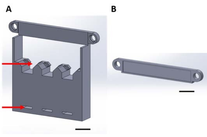
Figure 1: 3D printed pieces for handling functional devices during the gas-phase deposition in a vacuum desiccator. (A) The structure's base includes holders for 1 cm x 1 cm sample silicon squares (top arrow) and holes for securing to desiccator plate (bottom arrow). (B) The plate is used to secure the suspension of devices. From here onward, each piece in this figure will be referred to as either piece 1A or 1B. Scale bar = 1 cm. Please click here to view a larger version of this figure.
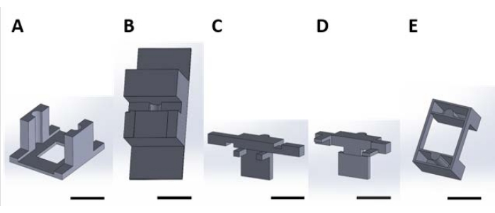
Figure 2: 3D printed pieces for handling functional devices for the surface reaction occurring in the aqueous solution. (A) Guide piece to be glued to the lid of the culture plate. (B) Benchtop pieces used to stabilize pieces (C) and (D) while assembling. (C) and (D) together secure the suspension of devices for placement in the well plate, and (E) further secures pieces (C) and (D) to the well plate lid. From here onward, individual pieces in each panel of this figure will be referred to as piece numbers corresponding to the panel number of this figure. Scale bar = 1 cm. Please click here to view a larger version of this figure.
All the coding files for 3D printing are provided in Supplementary Coding Files 1-16. The analysis provided in the Representative results is described using commercially acquired functional silicon planar electrode arrays (see Table of Materials).
1. Handling assembly for gas-phase deposition in a vacuum desiccator
NOTE: The assembled apparatus for handling and holding devices during gas-phase deposition is shown in Figure 3. Steps 1.1-1.8 describe the procedure required to place the devices into the apparatus for deposition (Figure 4A).

Figure 3: Assembly of 3D printed pieces for handling functional devices during gas-phase deposition. The assembly is pictured without samples to be coated. Screws and wing nuts are used to fasten pieces 1A and 2B together. Please click here to view a larger version of this figure.

Figure 4: Image of assembly and placement of samples to be coated. This scheme describes the handling of functional devices during gas-phase deposition secured within a vacuum desiccator. (A) Double-sided polyimide tape placed on piece 1A and foam tape placed on 1B. (B) Devices secured onto tape. (C) Screws and wing nuts are used to fasten pieces 1B to 1A, and the assembly is attached to the desiccator tray using zip cable ties (red arrows). (D) 1 cm x 1 cm silicon square samples are placed into respective holders. (E) The aluminum weigh dish and pressure gauge are placed into the desiccator in the orientation shown. Please click here to view a larger version of this figure.
- For surface treatment, acquire 1 cm x 1 cm square samples of the devices' substrate material.
- For silicon samples (selected for this protocol), cut the silicon wafer into 1 cm x 1 cm squares using a wafer dicing machine (see Table of Materials).
- Print or acquire pieces 1A (Figure 1A, Supplementary Coding File 1, Supplementary Coding File 2) and 1B (Figure 1B, Supplementary Coding File 3, Supplementary Coding File 4).
- Attach double-sided polyimide tape to piece 1A and attach 1/8" thick foam strip with one-side adhesive to piece 1B.
- Adhere the connector packaging of the device to the tape on piece 1A.
NOTE: The ideal orientation of the connector on the tape will leave the shank suspended over the edge, as shown in Figure 4B. - Secure piece 1A and piece 1B together (Figure 4C). Align the holes and secure using stainless steel screws and wing nuts (see Table of Materials).
- Using zip ties, fasten the assembly to the vacuum desiccator tray using the holes in the bottom of piece 1A as shown in Figure 4C.
- If applicable, place square material samples into the slits at the bottom of the frame (Figure 4D). Here, 1 cm x 1 cm square silicon wafer diced samples are used as an example.
NOTE: The exact material will need to match the substrate of the treated device, which will vary depending on the device. - Complete the gas-phase deposition by placing the solution into an appropriate receptacle within the vacuum desiccator opposite and in line with the secured assembly.
NOTE: Aluminum weigh dishes were used as receptacles for the (3-Aminopropyl)triethoxysilane (APTES) deposition, as an example here.- Place a vacuum gauge (see Table of Materials) within the desiccator to record the exact pressure. Position the port of the desiccator lid near the secured assembly and in line with the solution (Figure 4E).
NOTE: Further details regarding this method of gas-phase deposition are described in a previously published Reference49.
- Place a vacuum gauge (see Table of Materials) within the desiccator to record the exact pressure. Position the port of the desiccator lid near the secured assembly and in line with the solution (Figure 4E).
2. Handling assembly for surface reaction via aqueous solution
NOTE: The components and assembled apparatus for handling and holding devices during aqueous phase deposition and surface treatment are illustrated in Figures 5-7. The following steps will detail the procedure required to place the devices into the apparatus for deposition and treatment.

Figure 5: Assembly of 3D printed pieces for handling functional devices for the surface reaction occurring in aqueous solution. (A) Guide piece to be glued to the lid of the culture plate. (B) The benchtop piece was used to stabilize pieces (C) and (D) while assembling. (C) and (D) together secure the suspension of devices for placement in the well plate. (E) further secures pieces (C) and (D) to the well plate lid. Double-sided polyimide tape was placed on the lower portion of (C), and foam tape was placed on the lower portion of (D) (both boxed in red). Please click here to view a larger version of this figure.

Figure 6: Cell culture plate lid constructed with 6 guides (piece 2A). Please click here to view a larger version of this figure.

Figure 7: Sequence for securing and loading probes for solution reaction. The color of the parts was changed in this figure for clarity within the image. These are the same parts as Figure 5 and Figure 6. (A) Piece 2C is placed into piece 2B, and the device is secured to the taped portion of 2C. (B) Piece 2D fits into piece 2C to create an assembly that suspends the device shank. (C) The assembly of 2C, 2D, and the device is carefully positioned onto the lid of the well plate using the guide. (D) Piece 2E fits on top of the assembly to further secure the lid. Please click here to view a larger version of this figure.
- Construct a lid for the well plate to suspend the electrode array of the device in solution (Figure 6). This protocol describes the use of a 24-well plate.
- Cut rectangular holes 19 mm x 10.5 mm into the lid of the well plate using a laser cutter or manually with a box cutter. Match the number of holes to the number of devices desired for treatment.
NOTE: For ease of assembly, it is recommended to treat six devices per well plate, or at minimum, place holes over non-adjacent wells (Figure 6). - Print or acquire the appropriate number of guides (piece 2A (Figure 2A), Supplementary Coding File 5, Supplementary Coding File 6).
- Use cyanoacrylate adhesive to secure guides to the lid. Align the rectangular holes in the guides and lids while gluing to ensure the guide's rectangular hole is unobstructed, as shown in Figure 6.
- Cut rectangular holes 19 mm x 10.5 mm into the lid of the well plate using a laser cutter or manually with a box cutter. Match the number of holes to the number of devices desired for treatment.
- Fill the well plate with the desired solution at locations where treatment will occur. For example purposes, the solution comprises EDC and Sulfo-NHS (see Table of Materials) in MES buffer.
NOTE: The volume of the solution will depend on the electrode device's dimensions. For Michigan-style microelectrode arrays (see Table of Materials) with low-profile connectors of 8.6 mm and shank length of 3 mm, there is ~9 mm clearance50. Using 2 mL of solution will allow for the shank of the device to be fully submerged while keeping the remainder of the device out of the reaction solution.- If substrate samples are being used to confirm surface treatment, place square material samples in a well of the plate and submerge them in the reaction solution.
- Securely suspend the devices (see Table of Materials) in a well plate. The sequence is shown in Figure 7.
- Tape piece 2B (Figure 2B, Supplementary Coding File 7, Supplementary Coding File 8) to a benchtop (Figure 7A).
- Place double-sided polyimide tape to cover the base of piece 2C (Figure 2C, Supplementary Coding File 9, Supplementary Coding File 10).
- Place 1/8" foam tape with single-side adhesive to cover the base of piece 2D (Figure 2D, Supplementary Coding File 11, Supplementary Coding File 12).
- Fit piece 2C into the groove of piece 2B (Figure 7A).
- Adhere the connector packaging of the device onto the tape, oriented, so the length of the device shank is suspended (Figure 7B).
- Secure the device by sliding piece 2D (shown in orange in Figure 7) into piece 2C. This assembly effectively secures the device between the tool pieces (Figure 7B).
- Holding the edges of the assembly, carefully lift to remove from piece 2A.
- Fit the assembly into the lid by aligning the outward-facing semicircles on pieces 2C and 2D with the corresponding guides on piece 2A (shown in green in Figure 7C).
- Secure assembly placement by press-fitting piece 2E (Figure 2E) over the guides (shown in green in Figure 7D, Supplementary Coding File 13, Supplementary Coding File 14).
- For reactions that benefit from continuous mixing of the solution, agitate the well plate. Transfer the assembled well plate to a shaker table and run at speeds under 100 rpm.
- If multiple solution-based reactions or wash steps are desired, carefully transfer the lid to a new well plate with desired solution(s) distributed to the appropriate wells.
NOTE: Step 2.4 is optional. - Remove devices from the well plate.
- Tape piece 2B to a benchtop.
- Remove piece 2E from the lid.
- Carefully remove the assembly holding the device from the well plate.
- Orient the assembly, so that piece 2C faces the benchtop and piece 2D faces upward. The shank of the device needs to be parallel to the benchtop. Fit piece 2C of the assembly into piece 2B as was completed previously (step 2.3.4) when fitting together the assembly.
- Separate piece 2D from piece 2C by carefully pulling them apart. Apply slight pressure on the tabs of piece 2C into the bench to provide stability for this task.
NOTE: The tabs of 2C are longer than that of 2D to facilitate this handling. - Use forceps to hold onto the device's connector packaging to remove from the tape and transfer the device to the desired storage container.
To demonstrate the use of the handling components, the described methodology was implemented to adapt the immobilization of an oxidant mediator to activated silicon. The application of this chemistry to IMEs to reduce oxidative stress was devised by Potter-Baker et al. and demonstrated on non-functional silicon dummy probes40. This surface treatment immobilizes the antioxidant, MnTBAP, to UV/ozone activated silicon surface via amine functionalization followed by carbodiimide crosslinking chemistry51. The amine functionalization is completed via gas-phase deposition and the carbodiimide crosslinking chemistry via aqueous reaction. These experiments were conducted using commercially available Michigan-style microelectrode arrays and silicon square samples to allow for material analysis of the coating method (see Table of Materials).
First, amine functionalization was performed using the aminosilane, (3-Aminopropyl)triethoxysilane (APTES). The gas-phase deposition of APTES employed an adaption of methods described by Munief et al.49. The devices were securely suspended using the 3D printed tools following the described handling protocol for gas-phase treatment. Next, 400 µL of liquid APTES was placed into an aluminum dish within the vacuum desiccator. The desiccator lid was placed, and the vacuum was pulled to ~25 psi for 20 min. After 20 min, the vacuum was released. A fresh 400 µL of liquid APTES was placed into a new aluminum dish. The vacuum was pulled again to ~25 psi for an additional 20 min. After 20 min, the APTES was refreshed a second time, and the vacuum was held at ~25 psi for 24 h52. Following the amine functionalization, carbodiimide crosslinking chemistry was used to immobilize MnTBAP. Standard procedure using 1-[3-(Dimethylamino)propyl]-3-ethylcarbodiimide methiodide (EDC) and N-Hydroxysulfosuccinimide sodium salt (Sulfo-NHS) in 2-(N-Morpholino)ethanesulfonic acid (MES) buffer was employed as previously described40. The 3D-printed tools suspended the devices in wells containing the reaction solution.
Following the completion of the functionalization reactions, ellipsometry and x-ray photoelectron spectroscopy (XPS) was performed to confirm the presence of APTES (step 1) and MnTBAP (step 2), respectively. Silicon squares 1 cm x 1 cm were used to analyze each coating process step to validate successful APTES deposition and MnTBAP immobilization. Ellipsometry measurements taken from the center of 12 silicon samples produced a mean APTES layer thickness of 8.5 ± 1.02 Å, compared to the theoretical monolayer thickness of 7 Å. Results of XPS are provided in Table 1. Following the gas-phase APTES treatment, there is an increase in the percentage of the atomic concentrations of nitrogen and carbon, indicative of the chemical deposit. Following the solution phase immobilization process, these results demonstrate the presence of manganese, the element contributing to the activity of MnTBAP, which was undetectable before solution-phase immobilization.
| Modification | C (%) | N (%) | O (%) | Si (%) | Mn (%) | ||
| Plasma treated Si | 3.06 | 0.5 | 49.84 | 46.605 | 0 | ||
| APTES gas phase deposition | 13.63 | 3.2 | 43.98 | 39.2 | 0 | ||
| MnTBAP immobilized | 44.16 ± 3.94 | 5.33 ± 0.37 | 21.81 ± 1.30 | 21.81 ± 2.39 | 0.79 ± 0.07 | ||
Table 1: XPS analysis for sequential modifications to silicon. Values provided for the MnTBAP immobilization step are presented with a standard deviation for a sample size of 4.
The functionality of Michigan-style microelectrode arrays after the coating processes was assessed using electrical impedance spectroscopy (EIS)50. EIS was recorded for 20 total microelectrode channels across two devices. The channels included for the test were randomly selected and evenly distributed between the two devices (10 channels/device). The measurements were made using a potentiostat with a three-electrode setup. Measurements were completed for each channel three times before the coating process and three times after the coating process. The impedance magnitude at 1 kHz was 238 ± 10.22 kΩ and 237 ± 9.81 kΩ before and after the coating process, respectively. A pairwise t-test was selected to determine whether the coating process affected the channel impedance53. The device's impedance measurements present significant variance; thus, an analysis on the device level may lose an effect of the coating within the noise of manufacturing variability. A pairwise t-test between impedance magnitudes of the channels at 1 kHz before and after the coating process indicated no statistical difference (p > 0.937). The bode plot of a tested device is provided in Figure 8, displaying the results of 10-channel recordings before and after treatment. Images of the electrode array before and after the coating process are provided in Figure 9. Additional information regarding the instrumental details for the material analyses can be found in Supplementary File 1.

Figure 8: Bode plot displaying average electrochemical impedance measurements across one tested device (10 channels) before (gray) and after (red) the coating procedure. The bars represent the standard error of the mean. The impedance magnitude decreased with increasing frequency. The phase angle decreased with increasing frequency. Please click here to view a larger version of this figure.

Figure 9: Images of electrode array before (top) and after (bottom) the coating process. Scale bar = 50 µm. Please click here to view a larger version of this figure.
Supplementary File 1: Instrumental details for material analyses. Please click here to download this File.
Supplementary Coding Files 1-16: Please click here to download this File.
