We describe a procedure to optically trap micro-particles in nanoplasmonic optical lattice.
The plasmonic optical tweezer has been developed to overcome the diffraction limits of the conventional far field optical tweezer. Plasmonic optical lattice consists of an array of nanostructures, which exhibit a variety of trapping and transport behaviors. We report the experimental procedures to trap micro-particles in a simple square nanoplasmonic optical lattice. We also describe the optical setup and the nanofabrication of a nanoplasmonic array. The optical potential is created by illuminating an array of gold nanodiscs with a Gaussian beam of 980 nm wavelength, and exciting plasmon resonance. The motion of particles is monitored by fluorescence imaging. A scheme to suppress photothermal convection is also described to increase usable optical power for optimal trapping. Suppression of convection is achieved by cooling the sample to a low temperature, and utilizing the near-zero thermal expansion coefficient of a water medium. Both single particle transport and multiple particle trapping are reported here.
The optical trapping of micro-scale particles was originally developed by Arthur Askin in the early 1970s. Ever since its invention, the technique has been developed as a versatile tool for micro- and nanomanipulation1,2. Conventional optical trapping based on the far-field focusing principle is inherently limited by the diffraction in its spatial confinement, wherein the trapping force decreases dramatically (following an ~a3 law for a particle of radius a)3. To overcome such diffraction limits, researchers have developed near-field optical trapping techniques based on the evanescent optical field using plasmonic metallic nanostructures and, furthermore, the trapping of nanoscale objects down to single protein molecules has been demonstrated4,5,6,7,8,9,10,11. Moreover, the plasmonic optical lattice is created from arrays of periodic plasmonic nanostructures to confer long range transport of micro- and nanoparticles and multiple particle stacking11,12. One major obstacle to disrupt trapping in an optical lattice is photothermal convection and efforts have been made to elucidate its effects by several groups14,15,16,17. Using Green's function, Baffou et al. have calculated a temperature profile by modeling each plasmonic nanostructure as a point heater and then experimentally validated their model14. Toussant's group has also measured the plasmon-induced convection with particle velocimetry15. The author's group has also characterized both near-field and convectional transport and demonstrated an engineering strategy to suppress photothermal convection16,17.
Here we present the design of an optical setup and a detailed procedure specifically for trapping experiments with plasmonic optical lattice. The optical potential was created by illuminating an array of gold nanodiscs with a loosely focused Gaussian beam. A scheme to suppress the photothermal convection by cooling down the sample to a low temperature (~4 °C) for optimal trapping is also describe here17. Under Boussinesq approximation, an order of magnitude estimate for the natural convection velocity u is given by u ~L2 gβΔT / v, where L is the length scale of the heat source and ΔT is the temperature increase relative to the reference due to the heating. g and β are the gravitational acceleration and thermal expansion coefficient, respectively. At temperatures near 4 °C, the density of the water medium exhibits anomalous temperature dependence and this translates into a near-zero thermal expansion coefficient and, therefore, a vanishingly small photothermal convection.
1. Optical Setup
Note: The principle of the optical setup is illustrated in Figure 1.
2. Nanofabrication
3. Sample cooling system and its temperature calibration
NOTE: The sample cooling stage design is shown in Supplementary Figure 2.
4. Trapping of Microparticles
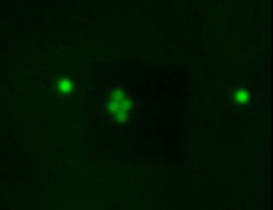
Single particle trajectories were recorded by a CCD camera in our experiment and the images were then processed with a custom program to extract each particle's trajectory16. Representative results are displayed in Figure 3 and Video 1 for micro-spheres with diameters of 2 µm. Multiple particle trappings inside the optical lattice were observed. Successive images extracted from a representative motion video of the particle are displayed in Figure 4. For microparticles of diameter 2 µm, one can see the clustering of microparticles formed a hexagonal close packed (hcp) structure. The sample can also be warmed up by turning off the TEC element; the observed trapped cluster would disperse due to photothermal convection.
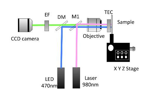
Figure 1. Schematic of the Optical Setup.
A Gaussian beam with wavelength of 980 nm is used to excite the plasmonic optical lattice sample to create trapping potential. A fiber-coupled laser diode of wavelength 980 nm goes through mirror (M1), gets loosely focused by a long working distance microscope objective, and excites the plasmonic sample. The fluorescent image is taken with same objective in conjunction with dichroic mirror (DM) and emission filter (EF) under the fluorescent excitation at 470 nm from light emitting diode light source. The excitation light at 980 nm for the plasmonic resonance is color coded 'pink' and the excitation and emission light for fluorescent imaging are color coded 'blue', and 'green', respectively. The motion is recorded with the CCD camera. Thermoelectrical cooling (TEC) is used to cool down the sample. Please click here to view a larger version of this figure.
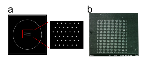
Figure 2. Nano Plasmonic Array Fabricated by E-Beam Lithography. (a) Marker design used to locate and align the sample in the e-beam writer. The dimensions of the outer white square are 22 mm x 22 mm, and the annular marker in the inset has an outer diameter of 150 µm and inner diameter of 50 µm. (b) A scanning electron microscope (SEM) image of a nanoplasmonic array. A simple square array of 22 x 22 nanodiscs is used and each unit cell contains one nanodisc of thickness 40 nm and diameter 550 nm with inter-disc distance 750 nm. Please click here to view a larger version of this figure.
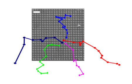
Figure 3. Single Particle Trajectories. The trajectories of the microparticles extracted using image processing are compiled using the centroid algorithm16 and displayed here. The optical power used for plasmonic resonance excitation at 980 nm is 5 mW. A scale bar of 2 µm is displayed. Please click here to view a larger version of this figure.
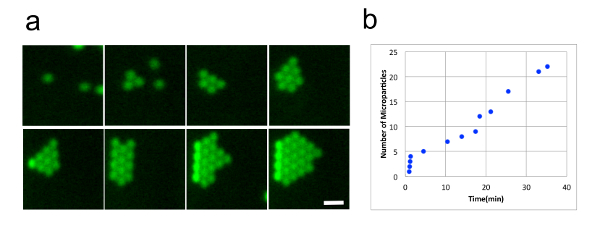
Figure 4. Image of a Cluster of Microparticles Trapped in Plasmonic Optical Lattice and Accumulation of Microparticles Over Time at an Optical Power of 5 mW. (a) Successive fluorescence images showing the accumulation of trapped microparticles forming clusters. A white scale bar of 4 µm is displayed. (b) Number of trapped microparticles versus time, extracted from (a). Please click here to view a larger version of this figure.
Video 1. Optical Trapping and Particle Accumulation of 2 µm Particles. The optical power used for plasmonic resonance excitation at 980 nm is 5 mW. Please click here to view this video. (Right-click to download.)
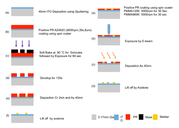
Supplementary Figure 1. Process Flow of Nanofabrication of Nanoplasmonic Array. Please click here to view a larger version of this figure.
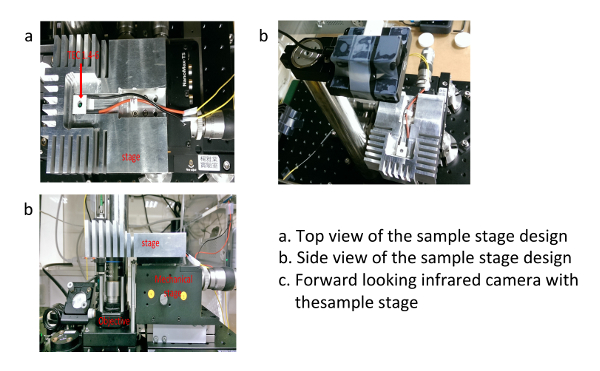
Supplementary Figure 2. Sample Cooling Stage Design. Please click here to view a larger version of this figure.
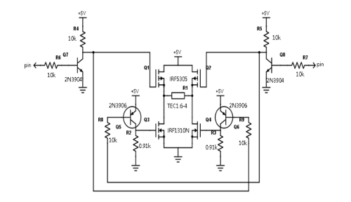
Supplementary Figure 3. Driver Circuit for Sample Cooling. Please click here to view a larger version of this figure.
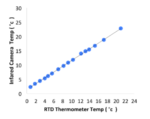
Supplementary Figure 4. Temperature Calibration between an rtd Thermometer and Forward-Looking Infrared Camera. Please click here to view a larger version of this figure.
The procedure described here enables the reader to reliably reproduce trapping on a daily basis. A general empirical guideline to design a usable optical lattice is to use a comparable size for plasmonic nanoarray, interdisc distance, and trapped particle size. Compared to a single, isolated plasmonic nanostructure, the optical lattice design in conjunction with the high optical power afforded by cooling the sample to ~4 °C used here greatly enhances the trapping probability. If well separated, plasmonic nanostructures are used as trapping sites, one needs to wait for a long time for the migration of microparticles into the effective trapping volume near the plasmonic nanostructures. Also, increasing the inter-disc distance critically diminishes the probability of particle accumulation. Note that one can also perform the trapping experiment with the plasmonic optical lattice at room temperature but the usable optical power will be very limited. Also, at low optical power, one needs to wait for a long time (~ 1 h) for the microparticle trapping event. Typically, we turn on the CCD camera to record the particle motion and pick up the trapping event within a few minutes. The applicable laser power is as high as 10 mW. At a high optical power, a large aggregation of microparticles can be observed.
The critical step for success in this work is to cool down the plasmonic on a fragile cover slip and simultaneously monitor the sample temperature. We have chosen the forward looking infrared camera to measure the temperature because such a non-contact measurement greatly reduces the chance of sample breakage. Alternatively, one can choose to glue on a small size thermometer and use it to measure the temperature in real time. The cooling system together with non-contact temperature measurement is generally applicable for optical microscopy at low temperatures.
Although the demonstration here is done with micron-sized particles, one can trap nanoparticles by scaling down both the size and spacing of the gold nanodiscs. So far, trapping of nanoparticles with diameters as small as 100 nm has been demonstrated19. This is, however, not the ultimate limit of the plasmonic optical lattice. Also, we have used a long working distance microscope objective to ease the mechanical design of the sample stage. Better resolution in imaging can be achieved by replacing it with an oil immersion microscope objective. By scaling down the dimensions of the plasmonic nanostructures, the trapping of even smaller nanoparticles should also be feasible.20,21
The authors have nothing to disclose.
Y. T. Y. would like to acknowledge funding support from the Ministry of Science and Technology under grant numbers MOST 105-2221-E-007-MY3 and from the National Tsing Hua University under grant numbers 105N518CE1 and 106N518CE1.
Thermoelectric cooling element | Thorlabs | TEC 1.4-6 | TEC element for sample cooling |
RTD thermometer | Omega Engineering | RTD Thermometer 969C | |
Forward looking infrared camera | FLIR | FLIR One | IR camera for temperature monitoring |
light emitting diode light source | Touchbright | Light source for illumination for fluorescent imaging | |
Long working distance objective | Olympus | LMPLFLN | For illuminating the sample and imaging |
Optical trap kit | Thorlabs | OTKB/M | |
Cover slip | thickness 0.17 mm | ||
Scanning electron microscope | Hitachi | SEM-Hitachi S3400N | |
Electron beam blanker | DEBEN | PCD beam blanker | the blanker is added to the scanning electron microscope |
Thermal evaporator | SYSKEY Technology | ||
Mask aligner | Karl Suss | MJB 3 | For marker fabrication |
Electron beam resist | Sigma Alrich | PMMA 120K | For e-beam lithography |
Electron beam resist | Sigma Alrich | PMMA 960K | For e-beam lithography |
Fluoresent labeled polystyrene microspheres | Polyscience | 2 um diameter | |
Bipolar transistor | Mouser | 2N3904 | quantity 2 for TEC driver circuit |
Bipolar transistor | Mouser | 2N3906 | quantity 2 for TEC driver circuit |
MOSFET power transistor | Mouser | IRF5305 | quantity 2 for TEC driver circuit |
MOSFET power transistor | Mouser | IRF131ON | quantity 2 for TEC driver circuit |
10 kOhm resistor | Mouser | quantity 6 for TEC driver circuit | |
910 Ohm resistor | Mouser | quantity 2 for TEC driver circuit | |
Photoresist | Microchemicals | AZ4620 | For marker fabrication |
Acetone | Sigma Alrich | For marker fabrication | |
Fluorescence Module for the OTKB/M, Metric Threads | Thorlabs | OTKB-FL/M | |
Fluorescent filter set | Thorlabs | MDF-FITC | For Fluorescein Isothiocyanate (FITC) |
Ultrasonic cleaner | Delta | DC150H | For the lift off step |