Anodization parameters for growth of the aluminum-oxide dielectric layer of zinc-oxide thin-film transistors (TFTs) are varied to determine the effects on the electrical parameter responses. Analysis of variance (ANOVA) is applied to a Plackett-Burman design of experiments (DOE) to determine the manufacturing conditions that result in optimized device performance.
Aluminum-oxide (Al2O3) is a low cost, easily processable and high dielectric constant insulating material that is particularly appropriate for use as the dielectric layer of thin-film transistors (TFTs). Growth of aluminum-oxide layers from anodization of metallic aluminum films is greatly advantageous when compared to sophisticated processes such as atomic layer deposition (ALD) or deposition methods that demand relatively high temperatures (above 300 °C) such as aqueous combustion or spray-pyrolysis. However, the electrical properties of the transistors are highly dependent on the presence of defects and localized states at the semiconductor/dielectric interface, which are strongly affected by the manufacturing parameters of the anodized dielectric layer. To determine how several fabrication parameters influence the device performance without performing all possible combination of factors, we used a reduced factorial analysis based on a Plackett-Burman design of experiments (DOE). The choice of this DOE permits the use of only 12 experimental runs of combinations of factors (instead of all 256 possibilities) to obtain the optimized device performance. The ranking of the factors by the effect on device responses such as the TFT mobility is possible by applying analysis of variance (ANOVA) to the obtained results.
Flexible, printed and large area electronics represent an emerging market that is expected to attract billions of dollars in investments in upcoming years. To achieve the hardware requirements for the new generation of smartphones, flat panel displays and internet-of-things (IoT) devices, there is a huge demand for materials that are lightweight, flexible and with optical transmittance in the visible spectrum without sacrificing speed and high performance. A key point is to find alternatives to amorphous silicon (a-Si) as the active material of the thin-film transistors (TFTs) used in the drive circuits of most of the current active-matrix displays (AMDs). a-Si has low compatibility to flexible and transparent substrates, presents limitations to large-area processing, and has a carrier mobility of about 1 cm2∙V-1∙s-1, which cannot meet the needs of resolution and refresh rate for next generation displays. Semiconducting metal oxides (SMOs) such as zinc oxide (ZnO)1,2,3, indium zinc oxide (IZO)4,5 and indium gallium zinc oxide (IGZO)6,7 are good candidates to replace a-Si as the active layer of TFTs because they are highly transparent in the visible spectrum, are compatible to flexible substrates and large area deposition and can achieve mobilities as high as 80 cm2∙V-1∙s-1. Moreover, SMOs can be processed in a variety of methods: RF sputtering6 , pulsed laser deposition (PLD)8, chemical vapor deposition (CVD)9, atomic layer deposition (ALD)10, spin-coating11, ink-jet printing12 and spray-pyrolysis13.
However, few challenges such as the control of intrinsic defects, air/UV stimulated instabilities and formation of semiconductor/dielectric interface localized states still need to be overcome to enable the large-scale manufacturing of circuits comprising SMO-based TFTs. Among the desired characteristics of high performance TFTs, one can mention the low power consumption, low operation voltage, low gate leakage current, threshold voltage stability and wideband frequency operation, which are extremely dependent on the gate dielectrics (and the semiconductor/insulator interface as well). In this sense, high-κ dielectric materials14,15,16 are particularly interesting since they provide large values of capacitance per unit area and low leakage currents using relatively thin films. Aluminum oxide (Al2O3) is a promising material for the TFT dielectric layer since it presents a high dielectric constant (from 8 up to 12), high dielectric strength, high electrical resistivity, high thermal stability and can be processed as extremely thin and uniform films by several different deposition/growth techniques15,17,18,19,20,21. Additionally, aluminum is the third most abundant element in the Earth’s crust, what means that it is easily available and relatively cheap compared to other elements used to produce high-k dielectrics.
Although deposition/growth of Al2O3 thin (below 100 nm) films can be successfully attained by techniques such as RF magnetron sputtering, chemical vapor deposition (CVD), atomic layer deposition (ALD), the growth by anodization of a thin metallic Al layer17,18,21,22,23,24,25,26 is particularly interesting for flexible electronics owing to its simplicity, low cost, low temperature, and film thickness control in nanometric scale. Besides, anodization has a great potential for roll-to-roll (R2R) processing, which can be easily adapted from processing techniques already being used at industrial level, permitting quick manufacturing upscaling.
Al2O3 growth by anodization of metallic Al can be described by the following equations
2Al + 3 / 2 02 → Al2O3 (1)
2Al + 3H2O → Al2O3 + 3H2 (2)
where the oxygen is provided by the dissolved oxygen in the electrolyte solution or by the adsorbed molecules at the film surface, whereas the water molecules are promptly available from the electrolyte solution. The anodized film roughness (which affects the TFT mobility due to carrier scattering at the semiconductor/dielectric interface) and the density of localized states at the semiconductor/dielectric interface (which affects the TFT threshold voltage and electrical hysteresis) are strongly dependent on anodization process parameters, to name a few: the water content, the temperature and the pH of the electrolyte24,27. Other factors related to the Al layer deposition (like evaporation rate and metal thickness) or to post-anodization processes (like annealing) can also influence the electrical performance of fabricated TFTs. The effect of these multiple factors on response parameters can be studied by varying each factor individually while keeping all other factors constant, which is an extremely time-consuming and inefficient task. Design of experiments (DOE), on the other hand, is a statistical method based on the simultaneous variation of multiple parameters, which permits the identification of the most significant factors on a system/device performance response by using a relatively reduced number of experiments28.
Recently, we have used multivariate analysis based on a Plackett-Burman29 DOE to analyze the effects of Al2O3 anodization parameters on the performance of sputtered ZnO TFTs18. The results were used to find the most significant factors for several different response parameters and applied to the optimization of the device performance changing only parameters related to the anodization process of the dielectric layer.
The current work presents the whole protocol for manufacturing TFTs using anodized Al2O3 films as gate dielectrics, as well a detailed description for the study of the influence of the multiple anodization parameters on the device electrical performance by using a Plackett-Burman DOE. The significance of the effects on TFT response parameters such as the carrier mobility is determined by performing analysis of variance (ANOVA) to the results obtained from the experiments.
The protocol described in the present work is separated into: i) preparation of the electrolytic solution for anodization; ii) substrate cleaning and preparation; iii) anodization process; iv) deposition of the TFT active layer and drain/source electrodes; v) TFT electrical characterization and analysis and vi) application of ANOVA to determine the significance of the manufacturing factors in the TFT mobility.
1. Preparation of the electrolytic solution for anodization
2. Substrate cleaning and preparation
3. Aluminum gate electrode evaporation
4. Anodization process of the aluminum layer
5. Deposition of the ZnO Active layer
6. Drain and source electrodes deposition
7. TFT electrical characterization
8. ANOVA and influence of design factors on device performance
Eight different aluminum oxide layer manufacture parameters were used as the fabrication factors which we used to analyze the influence on the TFT performance. These factors are enumerated in Table 1, where the corresponding “low” (-1) and “high” (+1) values for the two-level factorial DOE are presented.
For simplicity, each manufacturing factor was named by a capital letter (A, B, C, etc.) and the corresponding “low” or “high” level represented by -1 and +1, respectively. The Placket-Burman DOE matrix considering eight factors varying in two levels results 12 experimental runs, with the combination of levels given by Table 2.
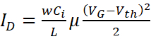
Each experimental run from Table 2 defines the fabrication conditions used to produce the Al2O3 layer used as the dielectric layer of a set of transistors with similar expected characteristics. Each set of transistors was electrically characterized by the TFT output and transfer curves. To obtain the mobility in the TFT saturation regime, we use the relationship between the channel current (ID) and the gate voltage:
(3)
where w is the channel width, L, the channel length, and Ci, the dielectric layer capacitance per unit area. The transfer curve for a TFT built according to manufacturing parameters given by run #3 from Table 2 is shown in Figure 1. The ID1/2 vs. VG curve is also depicted in Figure 1, allowing the evaluation of the TFT mobility (µ) from the slope of the curve and the threshold voltage (Vth) from the extrapolation of the linear region to the horizontal axis.
The values for the mobility for all built transistors according to the 12 runs parameters were computed in a table and used to feed input of the PB DOE assembled using the DOE/ANOVA analysis software (Chemoface). For each set of fabrication parameters, 6 replicated TFTs were built, resulting in 72 devices. By performing ANOVA, it is possible to rank the most significant factors, which can be graphically expressed using a Pareto chart of effects as shown in Figure 2a. Figure 2 presents the results from the analysis considering the TFT mobility as the response parameter. Similar analysis can be done for different device response parameters (on/off ratio, Vth, etc.). Figure 2b shows the table of effects and corresponding factor significance. The results demonstrate that the most significant factor for the TFT mobility is the final voltage (H) used during the anodization process. The final voltage is directly proportional to the dielectric layer thickness. The growth ratio is about 1.2 nm/V, which results, for example, in a 48 nm thick layer when using a final voltage of 40 V. Other significant factors were (in the following order): the Al evaporation rate (factor B), the thickness of the Al layer (factor A), the water content in the electrolyte (factor C) and the pH of the electrolyte (factor E). Moreover, all significant factors were found to be “negative”, which means that the TFT mobility decreases as the factor is changed from the “low” (-1) level to the “high” (+1) level given by Table 1. The significance of the manufacturing factors can be used as a direction to obtain optimized TFT performance for a particular response parameter (TFT mobility, in the current case).
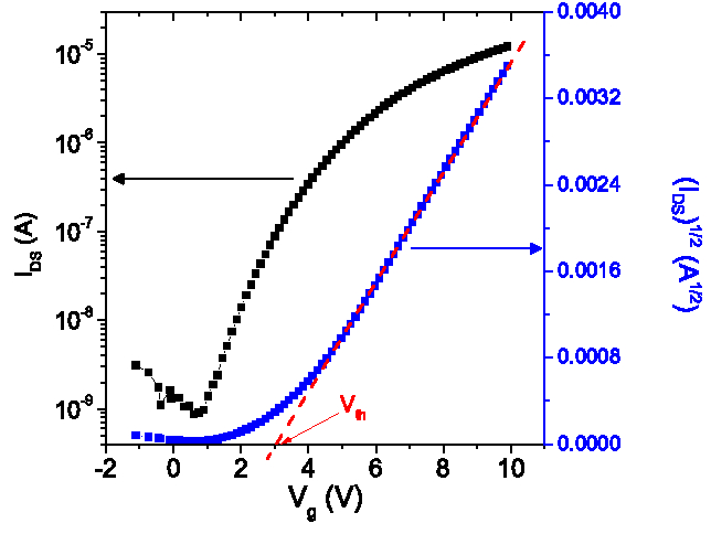
Figure 1: Transfer curve obtained from a TFT manufactured according to Run #3. The slope of the (IDS)1/2 vs. VG allows the determination of the TFT mobility and the intercept with the x-axis, the threshold voltage (Vth). Please click here to view a larger version of this figure.
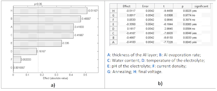
Figure 2: (a) Pareto chart of effects on the TFT mobility. (b) Table of effects and corresponding factor significance. Please click here to view a larger version of this figure.
Factors | Unit | “Low” value (-1) | “High” value (+1) | |||||||||
A | Thickness of Al-layer | nm | 60 | 200 | ||||||||
B | Al evaporation rate | Å /s | 5 | 15 | ||||||||
C | H2O content | % | 16 | 30 | ||||||||
D | Temperature of electrolyte | C | 40 | 60 | ||||||||
E | pH of the electrolytic solution | – | 6 | 5 | ||||||||
F | Current density | mA/cm2 | 0.45 | 0.65 | ||||||||
G | Annealing | C | No thermal treatment | Annealed at 150 oC | ||||||||
H | Final voltage | V | 30 | 40 |
Table 1: Manufacturing parameters of the aluminum oxide TFT dielectric layer. Each factor has a corresponding “low” (-1) or “high” (+1) value.
Run | A | B | C | D | E | F | G | H |
1 | -1 | -1 | -1 | -1 | -1 | -1 | -1 | -1 |
2 | 1 | -1 | 1 | 1 | -1 | 1 | 1 | 1 |
3 | -1 | -1 | -1 | 1 | -1 | 1 | 1 | -1 |
4 | 1 | -1 | -1 | -1 | 1 | -1 | 1 | 1 |
5 | 1 | 1 | -1 | 1 | 1 | 1 | -1 | -1 |
6 | -1 | 1 | -1 | 1 | 1 | -1 | 1 | 1 |
7 | 1 | 1 | 1 | -1 | -1 | -1 | 1 | -1 |
8 | -1 | -1 | 1 | -1 | 1 | 1 | -1 | 1 |
9 | 1 | -1 | 1 | 1 | 1 | -1 | -1 | -1 |
10 | 1 | 1 | -1 | -1 | -1 | 1 | -1 | 1 |
11 | -1 | 1 | 1 | -1 | 1 | 1 | 1 | -1 |
12 | -1 | 1 | 1 | 1 | -1 | -1 | -1 | 1 |
Table 2: Plackett-Burman (PB) design of experiment matrix
The anodization process used to obtain the dielectric has a strong influence on the performance of the TFTs fabricated, keeping constant all geometrical parameters and the fabrication parameters of the active. For the TFT mobility, which is one of the most important performance parameters for TFTs, it can vary more than 2 orders of magnitude by changing the manufacturing factors in the range given by Table I. Therefore, the careful control of the anodization parameters is of great importance when fabricating devices comprising anodized Al2O3 gate dielectrics. The presence of localized states due to charges/dipoles at the semiconductor/dielectric layer is one of the most significant causes of change in the device performance, especially for TFT mobility. Substrate cleaning is very important to avoid spurious variation of electrical parameters from device characterization. Use of alkaline residue-free detergent, use of deionized water for abundantly rinsing the substrates, use of analytical pure acetone and isopropanol for substrate cleaning and plasma cleaning are of extreme importance to assure the cleaning of the substrates and the reproducibility of the process. Rinsing and drying the substrates after the growth of the anodized layer have also be undertaken with extreme care. Control of the pH of the electrolyte, of the temperature of the electrolyte and stirring the electrolyte solution during anodization are also sources of random variation of the results. Contamination by dust also needs to be avoided by performing all steps inside a clean-room or a laminar flow cabinet. The type of acid used in the electrolyte also affects strongly the anodization process, however, because the effect of such factor cannot be properly quantified in a DOE, we used only tartaric acid, which results in good results for anodization.
The use of ANOVA to determine the significance of each manufacturing factor is an extremely powerful tool for device performance optimization. However, to obtain reliable results, it is essential to guarantee that the variance in the analyzed response parameter is due to factor variation and not by miscarried experimental procedure. A key point is to make as many replicates of each experimental run as possible. Although this increases the number of experiments that need to be performed, it increases the analysis reliability by increasing the number of degrees of freedom of the experimental design. A good strategy which was adopted in the current procedure was to produce 2 samples with 3 TFTs each. Therefore, the experimental run was repeated just once, but we had 6 replicated results from different devices. This also allowed to evaluate the variance for TFTs from the same substrate (same dielectric and semiconducting layers) and for TFTs from different substrates (different dielectric and semiconducting layers but fabricated according to the same procedure). If the variance for devices fabricated according to the similar manufacturing factors is low compared to the variance due to substantial changes in the manufacturing factors, the reproducibility of the process is acceptable.
As stressed before, Plackett-Burman design of experiments is very convenient for experiments with a high number of factors, since it permits a considerable reduction in the number of experiments. For 8 experimental factors, the number of experiments compared to a full-factorial design is reduced from 256 (28) to only 12. However, this reduction has the cost that the interaction between the factors cannot be evaluated. Therefore, for systems which the influence of the cross-factors is expected to be relevant, PBD is not the best option. A possibility is to use a PBD to screen the most significant factors and, in a second moment, to use a full-factorial design for the most significant factors from the PBD to determine the influence of the factor interactions.
The use of the experimental design software Chemoface30 in the analysis is optional and the results should not be dependent of it. All the calculations needed to determine the effects of the factors on the system response can be performed manually (extremely time-consuming), by a custom computer-aid script, or by other professional software such as Minitab or Design-Expert. However, Chemoface is a user-friendly and cost-free interface which is available for download without any restriction.
The current work demonstrates feasibility of manufacturing thin-film transistors comprising Al2O3 dielectric layer grown by anodization of metallic aluminum. This process can be easily extended to flexible substrates, allowing mass production of flexible electronic circuits. The use of Plackett-Burman design of experiments combined to ANOVA is a quick and powerful method to screen the influence of manufacturing factors in the device response, permitting the TFT performance optimization.
The authors have nothing to disclose.
The authors acknowledge the financial support from São Paulo Research Foundation – FAPESP – Brazil (grants 19/05620-3, 19/08019-9, 19/01671-2, 16/03484-7 and 14/13904-8) and Research Collaboration Program Newton Fund from Royal Academy of Engineering. Authors also acknowledge the technical support from B. F. da Silva, J.P. Braga, J.B. Cantuaria, G.R. de Lima and G.A. de Lima Sobrinho and Prof. Marcelo de Carvalho Borba’s group (IGCE/UNESP) for providing the filming equipment.
Acetone | LabSynth | A1017 | ACS reagent grade |
Aluminum (Al) Wire Evaporation | Kurt J. Lesker Company | EVMAL40060 | 1.5 mm (0.060") Dia.; 1lb; 99.99% |
Ammonium hydroxide solution | Sigma Aldrich | 338818 | ACS reagent, 28.0-30.0% NH3 basis |
Chemoface – Software to set a design of experiment (DOE) | Federal University of Lavras (UFLA), Brazil | Free software developed by Federal University of Lavras (UFLA), Brazil – http://www.ufla.br/chemoface/ | |
Cleaning detergent | Sigma Aldrich | Alconox | Alkaline detergent for substrate cleaning |
Ethylene glycol | Sigma Aldrich | 102466 | ReagentPlus, ≥99% |
Isopropanol | LabSynth | A1078 | ACS reagent grade |
Glass substrates | Sigma Aldrich | CLS294775X50 | Corning microscope slides, plain |
L-(+)-Tartaric acid | Sigma Aldrich | T109 | ≥99.5% |
Mechanical shadow mask for deposition of the sputtered ZnO active layer | Lasertools, Brazil | custom mask | 10 mm x 10 mm square. |
Mechanical shadow mask for TFT gate electrode | Lasertools, Brazil | custom mask | 25 mm long stripe, 3 mm wide. |
Mechanical shadow mask for TFT source/drain electrodes | Lasertools, Brazil | custom mask | 100 µm stripes, separated by 100 µm gap, overlapping of 5 mm |
Plasma cleaner | MTI | PDC-32G | Campact plasma cleaner with vacuum pump |
Sputter coating system | HHV | Auto 500 | RF sputtering system with thickness and deposition rate control |
Stiring plate | Sun Valley | MS300 | Stiring plate with heating control |
Thermal evaporator | HHV | Auto 306 | it has a high precision sensor for measure the thickness and rate of deposition of thin films |
Two-channel source-measuring unit | Keithley | 2410 | Keithley model 2410 or similar/for anodization process |
Two-channel source-measuring unit | Keithley | 2612B | Dual channel source-measure unit (SMU) for TFT measurements |
Ultrasonic bath | Soni-tech | Soni-top 402A | Ultrasonic bath with heating control |
Zinc Oxide (ZnO) Sputtering Targets | Kurt J. Lesker Company | EJTZNOX304A3 | 3.0" Dia. x 0.250" Thick; 99.9% |