Summary

电化学腐蚀和电子碰撞电离夏普场发射点的表征

Published: July 12, 2016
doi:

Summary

A method for electrochemically etching field emission tips is presented. Etching parameters are characterized and the operation of the tips in field emission mode is investigated.

Abstract

A new variation of the drop-off method for fabricating field emission points by electrochemically etching tungsten rods in a NaOH solution is described. The results of studies in which the etching current and the molarity of the NaOH solution used in the etching process were varied are presented. The investigation of the geometry of the tips, by imaging them with a scanning electron microscope, and by operating them in field emission mode is also described. The field emission tips produced are intended to be used as an electron beam source for ion production via electron impact ionization of background gas or vapor in Penning trap mass spectrometry applications.

Introduction

尖锐尖端或点已长期显微镜应用,如场离子显微镜(FIM)1和扫描隧道显微镜(STM)2,和一系列的用于制造各种材料的尖锐尖端技术中使用已开发了3。这些尖头还可以通过施加高电压,以它们作为场致发射点(前置机)动作,并作为一个方便的电子束源。如源的一个应用是通过电子轰击电离(EII)离子的生产。该FEP是在由热发射体产生的温度波动是不期望的应用中是特别有利的。例如,通过背景气体或蒸气的EII离子生产高精度潘宁陷阱4,5。

用于制造前置机一个简单的方法是电化学蚀刻钨棒在氢氧化钠(NaOH)溶液。这种技术相对简单,以便实现具有适度的设备,并已被证明是相当重复,可靠。许多方法在文献中有描述和改进这些技术继续出现6。在这里,我们描述了钨提示在NaOH溶液中电化学腐蚀的方法。我们的方法是片晶落客技术7,8的变化和浮层技术9,10。这两种方法,如它能够生产的从单个蚀刻过程两个尖端。用于蚀刻的尖端的实验装置的图象示于图1。
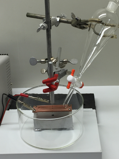
图1
图1.蚀刻设备。用于钨棒用NaOH溶液的电化学蚀刻的实验装置的照片。 此处查看该图的放大版本。

在NaOH水溶液碱钨的电化学蚀刻经由一个两阶段过程中发生。首先,中间氧化钨形成​​,并且第二,这些氧化物是非电化学溶解形成可溶性钨阴离子。这个过程的描述,以简化形式,由两个反应

(1)W + 6OH →WO 3(s)+ 3H 2 O + 6e中 ,和

(2)WO 3(s)+ 2OH →WO 4 2- + H 2 O

蚀刻电流和所用的NaOH溶液的摩尔浓度影响通过钨棒以蚀刻所需要的时间和电压。在这些效应的研究介绍和讨论。更重要的是,蚀刻参数有场发射模式上的提示的几何形状,并且作为这样的效果,对它们的操作。的几何通过将它们与扫描型电子显微镜(SEM)成像,我们产生的提示进行了表征。这些图像可以被用来估计,例如,尖端半径。此外,该提示是在场致发射模式通过施加通常几百伏的负电压到几千伏给他们,并监测所产生的电子发射电流。场致发射电流之间的关系,I和施加的偏置电压V,可以通过福勒-诺德海姆方程11所描述

(3)I = AV 2ë-Cr EFF / V,

其中r eff是尖的有效半径,A是常数,C是所述第二福勒-诺德海姆恒定公式9 ,其中B = 6.83 eV的 3/2 V /纳米,030eq11.jpg“/>是钨的功函数( 11式 ≈4.5电子伏特),k为取决于几何因素(K≈5),12式是诺德海姆图像校正项( 12式 ≈1)12。因此,前端的有效半径可以通过测量电子电流作为偏置电压的函数来确定。具体地,它可以从LN的一个所谓的福勒-诺德海姆(FN)情节(I / V 2)1 / V的斜率来获得。

Protocol

1.电化学腐蚀 实验装置 仪器 注意:电化学蚀刻设置需要一个标准0 – 30伏直流(DC)台式电源和相应的电缆,分液漏斗,一个宽基底玻璃烧杯中,标准杆和效用钳电绝缘夹具。小螺丝,绝缘支座,和鳄鱼夹也将被要求。其他项目,下面描述并且在图1中的蚀刻装置的图所示,必须制造。 从约100毫米长直径6毫米铝棒使钨杆保持器。钻一…

Representative Results

研究腐蚀参数 在蚀刻工艺期间的电源是恒流模式操作。所需的电压作为钨棒蚀刻掉(由于在杆的阻力的增加),以略微保持这个恒定电流增大。目前几乎降到零当尖端通过蚀刻一路。一个小的电流继续由于流动的事实,上部前端仍然与蚀刻溶液接触。的电流和电压作为蚀刻工艺期间作为时间函数作图示于图…

Discussion

我们已经描述了简单的程序,以在一个NaOH溶液电化学蚀刻尖锐场发射点(前置机),并通过场发射模式操作它们来测试前置机。所描述的蚀刻过程是现有技术-薄片下车技术7,8和浮动层技术9,10的变化。但是,我们发现这是更加方便和可靠比上述的方法来实现。

在开始蚀刻过程,以最小化生产具有毛的变形, 例如,一个弯曲的末端,如在图2

Declarações

The authors have nothing to disclose.

Acknowledgements

We acknowledge the services of Stanley Flegler, Carol Flegler, and Abigail Tirrell at the MSU Center for Advanced Microscopy. We thank Ray Clark and Mark Wilson for technical assistance with the set-up of the electrochemical etching apparatus. Earlier contributions from Anne Benjamin, Georg Bollen, Rafael Ferrer, David Lincoln, Stefan Schwarz and Adrian Valverde, and technical assistance from John Yurkon are also acknowledged. This work was partially supported by the National Science Foundation contract no. PHY-1102511 and PHY-1307233, Michigan State University and the Facility for Rare Isotope Beams, and Central Michigan University.

Materials

Tungsten Rod 0.020" x 12" ESPI Metals http://www.espimetals.com/index.php/online-catalog/467-Tungsten  3N8 Purity
NaOH salt Cole-Parmer Item # WU-88404-71 100 g
Separatory funnel Cole-Parmer Item# WU-34506-03 250 mL 
DC Power supply BK Precision 1672 Triple Output 0 – 32 V, 0 – 3 A DC Power Supply
Acetone Cole-Parmer Item# WU-88000-68 500 mL
Data Acquisition Card National Instruments NI PXI-6221 16 AI, 24 DIO, 2 AO
Relay Magnecraft 276 XAXH-5D 7 A, 30 V DC Reed Relay
6-way 6" conflat flange cross Kurt J Lesker C6-0600
6" to 2-3/4" conflat zero length reducer flange  (x3) Kurt J Lesker RF600X275
2-3/4" conflat flange SHV feedthrough Kurt J Lesker IFTSG041033
2-3/4" conflat flange BNC feedthrough Kurt J Lesker IFTBG042033
2-3/4" conflat flange linear feedthrough MDC 660006, REF# BLM-275-2
6" conflat flange blankoff Kurt J Lesker F0600X000N
6" conflat flange window Kurt J Lesker VPZL-600
HV Power supply Keithley Instruments Keithley Model #2290-5 0 – 5 kV DC HV Power Supply
Picoammeter Keithley Instruments Keithley Model #6485
Faraday Cup Beam Imaging Solutions Model FC-1 Faraday Cup

Referências

  1. Muller, E. W., Bahadur, K. Field Ionization of Gases at a Metal Surface and the Resolution of the Field Ion Microscope. Phys. Rev. 102, 624 (1956).
  2. Binnig, G., Rohrer, H. Scanning Tunneling Microscopy. Helv. Phys. Acta. 55, 726-735 (1982).
  3. Melmed, A. J. The art and science and other aspects of making sharp tips. J. Vac. Sci. Technol. B. 9, 601-608 (1990).
  4. Shi, W., Redshaw, M., Myers, E. G. Atomic masses of 32,33S, 84,86Kr, and 129,132Xe with uncertainties 0.1 ppb. Phys. Rev. A. 72, 022510 (2005).
  5. Van Dyck, R. S., Zafonte, S. L., Van Liew, S., Pinegar, D. B., Schwinberg, D. B. Ultraprecise Atomic Mass Measurement of the α particle and 4He. Phys. Rev. Lett. 92, 220802 (2004).
  6. Hobara, R., Yoshimoto, S., Hasegawa, S., Sakamoto, K. Dynamic electrochemical-etching technique for tungsten tips suitable for multi-tip scanning tunneling microscopes. e-J. Surf. Sci. Nanotechnol. 5, 94-98 (2007).
  7. Klein, M., Schwitzgebel, G. An improved lamellae drop-off technique for sharp tip preparation in scanning tunneling microscopy. Rev. Sci. Instrum. 68, 3099-3103 (1997).
  8. Kerfriden, S., Nahlé, A. H., Campbell, S. A., Walsh, F. C., Smith, J. R. The electrochemical etching of tungsten STM tips. Electrochim. Acta. 43, 1939-1944 (1998).
  9. Lemke, H., Göddenhenrich, T., Bochem, H. P., Hartmann, U., Heiden, C. Improved microtips for scanning probe microscopy. Rev. Sci. Instrum. 61, 2538-2538 (1990).
  10. Song, J. P., Pryds, N. H., Glejbøl, K., Mørch, K. A., Thölén, A. R., Christensen, L. N. A development in the preparation of sharp scanning tunneling microscopy tips. Rev. Sci. Instrum. 64, 900-903 (1993).
  11. Fowler, R. H., Nordheim, L. Electron Emission in Intense Electric Fields. Proc. R. Soc. Lond. A. , 119-173 (1928).
  12. Kim, Y. -. G., Choi, E. -. H., Kang, S. -. O., Cho, G. Computer-controlled fabrication of ultra-sharp tungsten tips. J. Vac. Sci. Technol. B. 16, 2079 (1998).
  13. Brown, K. L., Tautfest, G. W. Faraday-Cup Monitors for High-Energy Electron Beams. Rev. Sci. Instrum. 27, 696 (1956).
  14. Redshaw, M., et al. Fabrication and characterization of field emission points for ion production in Penning trap applications. Int. J. Mass Spectrom. 379, 187-193 (2015).
  15. Ibe, J. P., et al. On the electrochemical etching of tips for scanning tunneling microscopy. J. Vac. Sci. Technol. A. 8, 3570 (1990).
  16. Ekvall, I., Wahlström, E., Claesson, D., Olin, H., Olsson, E. Preparation and characterization of electrochemically etched W tips for STM. Meas. Sci. Technol. 10, 11-18 (1999).
  17. Schiller, C., Koomans, A. A., van Rooy, T. L., Schönenberger, C., Elswijk, H. B. Decapitation of tungsten field emitter tips during sputter sharpening. Surf. Sci. 339, L925-L930 (1995).
check_url/pt/54030?article_type=t

Play Video

Citar este artigo
Van Well, T. L., Redshaw, M., Gamage, N. D., Kandegedara, R. M. E. B. Electrochemical Etching and Characterization of Sharp Field Emission Points for Electron Impact Ionization. J. Vis. Exp. (113), e54030, doi:10.3791/54030 (2016).

View Video