Summary

金属補導電気化学ナノインプリンティングの多孔質および固体シリコンウエハー

Published: February 08, 2022
doi:

Summary

20nm以下の形状精度を持つ3Dマイクロスケールの特徴を固体および多孔質シリコンウエハーに金属アシストした化学インプリンティング用プロトコルが提示されています。

Abstract

金属アシスト電気化学刷り込み(Mac-Imprint)は、金属アシスト化学エッチング(MACE)とナノインプリントリソグラフィーの組み合わせで、単結晶群IV(例えば、Si)およびIII-V(例えば、GaAs)半導体(例えば、GaAs)の半導体を直接パターニングすることができる。このプロセスの間に、貴金属触媒で被覆された再利用可能なスタンプは、フッ化水素酸(HF)および過酸化水素(H2O2)混合物の存在下でSiウエハと接触し、金属半導体接触界面でSiの選択的エッチングにつながります。このプロトコルでは、2つのMac-インプリント構成で適用されるスタンプと基板の調製方法について議論します: (1) 固体触媒を用いた多孔質Si Mac-インプリント;(2)多孔質触媒を有する固体Siマックインプリント。このプロセスは高いスループットで、サブ20 nm解像度でセンチメートルスケールの並列パターン化が可能です。また、1回の操作で低い欠陥密度と大面積パターニングを提供し、深い反応性イオンエッチング(DRIE)などのドライエッチングの必要性を回避します。

Introduction

半導体の三次元マイクロ・ナノスケールのパターニングとテクスチャ化により、光電子工学1,2、フォトニクス3、反射防止表面4、超疎水性、自己洗浄面など、さまざまな分野で多くの用途に対応できます。ソフトリソグラフィと20nm以下の解像度のナノインプリンティングリソグラフィにより、高分子フィルムのプロトタイピングと大量生産の3Dおよび階層パターンが成功しました。しかし、このような3D高分子パターンをSiに移すには、反応性イオンエッチング時のマスクパターンのエッチング選択性が必要であり、したがってアスペクト比が制限され、スカラップ効果による形状の歪みや表面粗さを誘導する7,8

多孔質のSiウエハース10,11と固体GaAsウエハース12,13,14の平行および直接パターン化のために、Mac-Imprintと呼ばれる新しい方法が達成されました。Mac-インプリントは、HFと酸化剤(例えば、Si Mac-Imprintの場合はH2O2)で構成されるエッチング液(ES)の存在下で、3D特徴を有する基板と貴金属被覆スタンプとの接触を必要とする接触式ウェットエッチング技術である。エッチングの間、2つの反応が同時に15,16に起こる:陰極反応(すなわち、貴金属でのH2O2還元、その間に正電荷キャリア[穴]が生成され、その後Si17に注入される)と陽極反応(すなわち、Si溶解、穴が消費される間)。十分な時間を経て、スタンプの3DフィーチャがSiウエハにエッチングされます。Mac-Imprintは、高スループット、ロールツープレートおよびロールツーロールプラットフォーム、非晶質、単結晶および多結晶SiおよびIII-V半導体との互換性など、従来のリソグラフィ法に比べて多くの利点を有します。Mac-インプリントスタンプは複数回再利用できます。さらに、この方法は、現代の直接書き込み方法と互換性のあるサブ20 nmエッチング解像度を提供することができます。

高忠実度の刷り込みを達成するための鍵は、エッチングフロント(すなわち、触媒と基板との接触界面)への拡散経路である。Azeredoら.9 の研究は、ES拡散が多孔質Siネットワークを介して有効であることを最初に実証した。Torralba et al.18は、固体Si Mac-Imprintを実現するために、多孔質触媒を介してES拡散が可能であることを報告した。Bastide et al.19 およびSharstniouら.20 は、ES拡散に対する触媒の空隙率の影響をさらに調べた。このように、Mac-インプリントの概念は、異なる拡散経路を持つ3つの構成でテストされています。

第1の構成では、触媒および基質は固体であり、初期拡散経路を提供しない。反応性拡散の欠如は、触媒-Si界面の端の周りの基板上の多孔質Siの層を形成するインプリンティング中の二次反応をもたらす。反応物は、その後枯渇し、反応が停止し、スタンプと基板の間で識別可能なパターン転送忠実度を生み出さない。第2および第3の構成において、拡散経路は、基板(すなわち、多孔質Si)または触媒(すなわち、多孔質金)に導入された多孔性ネットワークを介して可能であり、高いパターン移動精度が得られます。したがって、多孔質材料を介した大量輸送は、接触界面への反応物および反応生成物の接触インタフェースからの拡散を可能にする上で重要な役割を果たす9,18,19,20。3 つの構成の概略を図 1 に示します。

Figure 1
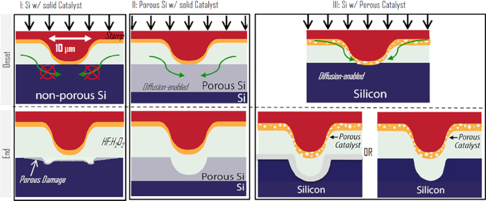
図 1: Mac インプリント構成の概略図 この図は、基材(すなわち、II:多孔質Si)またはスタンプ(すなわち、ケースIII:多孔質金からなる触媒薄膜)を介して反応種の拡散を可能にする多孔質材料の役割を強調する。 この図の大きなバージョンを表示するには、ここをクリックしてください。

本稿では、スタンプ調製や基板前処理、及びMac-インプリント自体を含む、Mac-インプリントプロセスについて徹底的に議論する。プロトコル内の基質前処理部には、ドライエッチングおよび基質陽極化によるSiウエハー洗浄およびSiウエハパターニング(任意)が含まれる。また、スタンプ準備部はいくつかの手順に細分化されます: 1) SiマスターモールドのPDMSレプリカ成形;2)PDMSパターンを転送するためにフォトレジスト層のUVナノインプリント;3)触媒層は、後に脱合金(任意)を続けてマグネトロンスパッタリングを介して堆積する。最後に、Mac-Imprint セクションでは、Mac-Imprint の結果(つまり、Si サーフェス 3D 階層パターン化)と共に Mac-Imprint のセットアップが表示されます。

Protocol

注意:適切な安全慣行と個人的な保護具(例えば、ラボコート、手袋、安全眼鏡、クローズドツシューズ)を使用してください。この手順は、非常に危険な化学物質であり、追加の個人的な保護具(すなわち、顔の盾、天然ゴムエプロン、および手、手首、前腕を覆うニトリル手袋の第2のペア)を必要とするHF酸(48%重量)を利用します。 1. マックインプリント用スタンプの準備</p…

Representative Results

走査型電子顕微鏡(SEM)画像、光学顕微鏡スキャン(図9)、および原子間力顕微鏡(AFM)スキャン(図10)を得て、Mac-ImprintスタンプおよびインプリントされたSi表面の形態学的性質を研究するために得られた。また、インプリントされた固体Siの断面プロファイルを、使用した多孔質Auスタンプのそれと比較した(図10</s…

Discussion

Mac-Imprintスタンプとプレパターン化されたSiチップ(p型、100方向、1〜10オーム∙cm)を、それぞれプロトコルのセクション1および2に従って調製した。3D階層パターンを含むスタンプを持つプレパターン化されたSiチップのMac-インプリントは、プロトコルのセクション3に従って行われた(図9)。図9aに示すように、Mac-Imprintの異なる構成が適?…

Declarações

The authors have nothing to disclose.

Acknowledgements

我々は、この研究に関する洞察についてケン・スー博士(ルイビル大学)を認める。イリノイ大学フレデリック・ザイツ研究所、そしてメモリアムでは、スタッフのスコット・マクラーレン。アリゾナ州立大学のルロイ・アイリング固体科学センター;そして、ビスグローブ学者賞の下で科学財団アリゾナ州。

Materials

Acetone, >99.5%, ACS reagent Sigma-Aldrich 67-64-1 CAUTION, chemical
Ammonium fluoride, >98%, ACS grade Sigma-Aldrich 12125-01-8 CAUTION, hazardous
Ammonium hydroxide solution, 28-30%, ACS reagent Sigma-Aldrich 1336-21-6 CAUTION, hazardous
AZ 400K developer Microchemicals AZ 400K CAUTION, chemical
BenchMark 800 Etch Axic BenchMark 800 Reactive ion etching
Chromium target, 2" x 0.125", 99.95% purity ACI alloys ADM0913 Magnetron sputter chromium target
CTF 12 Carbolite Gero C12075-700-208SN Tube furnace
Desiccator Fisher scientific Chemglass life sciences CG122611 Desiccator
F6T5/BLB Eiko F6T5/BLB 6W UV bulb
Gold target, 2" x 0.125", 99.99% purity ACI alloys N/A Magnetron sputter gold target
Hotplate KW-4AH Chemat tecnologie KW-4AH Leveled hotplate with uniform temperature profile
Hydrofluoric acid, 48%, ACS reagent Sigma-Aldrich 7664-39-3 CAUTION, extremly hazardous
Hydrogen peroxide, 30%, ACS reagent Fisher Chemical 7722-84-1 CAUTION, hazardous
Isopropyl alcohol, >99.5%, ACS reagent LabChem 67-63-0 CAUTION, chemical
MLP-50 Transducer Techniques MLP-50 Load cell
Nitric acid, 70%, ACS grade SAFC 7697-37-2 CAUTION, hazardous
NSC-3000 Nano-master NSC-3000 Magnetron sputter
Potassium hydroxide, 45%, Certified Fisher Chemical 1310-58-3 CAUTION, chemical
Rocker 800 vacuum pump, 110V/60Hz Rocker 1240043 Oil-free vacuum pump
Silicon master mold NILT SMLA_V1 Silicon chip with pattern
Silicon wafers, prime grade University wafer 783 Si wafer
Silver target, 2" x 0.125", 99.99% purity ACI alloys HER2318 Magnetron sputter silver target
SP-300 BioLogic SP-300 Potentiostat
SPIN 150i Spincoating SPIN 150i Spin coater
SPR 200-7.0 positive photoresist Microchem SPR 220-7.0 CAUTION, chemical
Stirring hotplate Thermo scientific Cimarec+ SP88857100 General purpose hotplate
SU-8 2015 negative photoresist Microchem SU-8 2015 CAUTION, chemical
SYLGARD 184 Silicone elastomere kit DOW 4019862 CAUTION, chemical
T-LSR150B Zaber Technologies T-LSR150B-KT04U Motorized linear stage
Trichloro(1H,1H,2H,2H-perfluorooctyl)silane (PFOCS), 97% Sigma-Aldrich 78560-45-9 CAUTION, hazardous

Referências

  1. Ning, H., et al. Transfer-Printing of Tunable Porous Silicon Microcavities with Embedded Emitters. ACS Photonics. 1 (11), 1144-1150 (2014).
  2. Hirschman, K. D., Tsybeskov, L., Duttagupta, S. P., Fauchet, P. M. Silicon-based light emitting devices integrated into microelectronic circuits. Nature. 384, 338-341 (1996).
  3. Cho, J., et al. Nanoscale Origami for 3D Optics. Small. 7 (14), 1943-1948 (2011).
  4. Azeredo, B. P., et al. Silicon nanowires with controlled sidewall profile and roughness fabricated by thin-film dewetting and metal-assisted chemical etching. Nanotechnology. 24 (22), 225305-225312 (2013).
  5. Lin, C., Tsai, M., Wei, W., Lai, K., He, J. Packaging Glass with a Hierarchically Nanostructured Surface: a universal method to achieve selfcleaning omnidirectional solar cells. ACS Nano. 10 (1), 549-555 (2016).
  6. Park, K. C., et al. Nanotextured Silica Surfaces with Robust Superhydrophobicity and Omnidirectional Broadband Supertransmissivity. ACS Nano. 6 (5), 3789-3799 (2012).
  7. Kim, J., Joy, D. C., Lee, S. Controlling resist thickness and etch depth for fabrication of 3D structures in electron-beam grayscale lithography. Microelectronics Engineering. 84 (12), 2859-2864 (2007).
  8. Deng, S., Zhang, Y., Jiang, S., Lu, M. Fabrication of three-dimensional silicon structure with smooth curved surfaces. Journal of Micro/Nanolithography, MEMS, and MOEMS. 15 (3), 0345031-0345036 (2016).
  9. Azeredo, B. P., Lin, Y., Avagyan, A., Sivaguru, M., Hsu, K. Direct Imprinting of Porous Silicon via Metal-Assisted Chemical Etching. Advanced Functional Materials. 26 (17), 2929-2939 (2016).
  10. Azeredo, B., Hsu, K., Ferreira, P. M. Direct Electrochemical Imprinting of Sinusoidal Linear Gratings into Silicon. The American Society of Mechanical Engineers – International Manufacturing Science and Engineering Conference. , 1-6 (2016).
  11. Li, H., Niu, J., Wang, G., Wang, E., Xie, C. Direct Production of Silicon Nanostructures with Electrochemical Nanoimprinting. ACS Applied Electronic Materials. 1 (7), 1070-1075 (2019).
  12. Kim, K., Ki, B., Choi, K., Lee, S., Oh, J. Resist-Free Direct Stamp Imprinting of GaAs via Metal-Assisted Chemical Etching. ACS Applied Materials & Interfaces. 11 (14), 13574-13580 (2019).
  13. Zhang, J., et al. Contact electrification induced interfacial reactions and direct electrochemical nanoimprint lithography in n-type gallium arsenate wafer. Chemical Science. 8, 2407-2412 (2017).
  14. Zhan, D., et al. Electrochemical micro/nano-machining: principles and practices. Chemical Society Reviews. 46 (5), 1526-1544 (2017).
  15. Li, X., Bohn, P. W. Metal-assisted chemical etching in HF / H2O2 produces porous silicon. Applied Physics Letters. 77 (16), 2572-2574 (2000).
  16. Chartier, C., Bastide, S., Levy-Clement, C. Metal-assisted chemical etching of silicon in HF – H2O2. Electrochimica Acta. 53, 5509-5516 (2008).
  17. Chattopadhyay, S., Li, X., Bohn, P. W. In-plane control of morphology and tunable photoluminescence in porous silicon produced by metal-assisted electroless chemical etching. Journal of Applied Physics. 91 (9), 6134-6140 (2002).
  18. Torralba, E., et al. 3D patterning of silicon by contact etching with anodically biased nanoporous gold electrodes. Electrochemistry Communications. 76, 79-82 (2017).
  19. Bastide, S., et al. 3D Patterning of Si by Contact Etching With Nanoporous Metals. Frontiers in Chemistry. 7, 1-13 (2019).
  20. Sharstniou, A., Niauzorau, S., Ferreira, P. M., Azeredo, B. P. Electrochemical nanoimprinting of silicon. Proceedings of the National Academy of Sciences. 116 (21), 10264-10269 (2019).
  21. Niauzorau, S., Ferreira, P., Azeredo, B. Synthesis of Porous Noble Metal Films with Tunable Porosity by Timed Dealloying. The American Society of Mechanical Engineers – International Manufacturing Science and Engineering Conference. , 1-4 (2018).
  22. Geyer, N., et al. Model for the Mass Transport During Metal-Assisted Chemical Etching with Contiguous Metal Films As Catalysts. The Journal of Physical Chemistry C. 116 (24), 13446-13451 (2012).
  23. Li, L., Liu, Y., Zhao, X., Lin, Z., Wong, C. Uniform Vertical Trench Etching on Silicon with High Aspect Ratio by Metal-Assisted Chemical Etching Using Nanoporous Catalysts. ACS Applied Materials and Interfaces. 6 (1), 575-584 (2014).
check_url/pt/61040?article_type=t

Play Video

Citar este artigo
Sharstniou, A., Niauzorau, S., Junghare, A., Azeredo, B. P. Metal-Assisted Electrochemical Nanoimprinting of Porous and Solid Silicon Wafers. J. Vis. Exp. (180), e61040, doi:10.3791/61040 (2022).

View Video