Summary

N极性InAlN阻高电子迁移率晶体管的等离子体辅助分子束外延

Published: November 24, 2016
doi:

Summary

分子束外延用来生长N极性InAlN阻高电子迁移率晶体管(HEMT器件)。在光滑,组成均匀InAlN层和HEMT的晶圆准备控制层生长条件和外延结构的结果与流动性高达1750厘米2 / V∙秒。

Abstract

等离子体辅助分子束外延非常适合于III族氮化物薄膜和异质的具有高品质的高电子迁移率晶体管(HEMT器件)需要平滑,突变接口外延生长。的过程提出了N极性InAlN HEMT器件的生长,包括晶圆制备和缓冲层,所述InAlN阻挡层的AlN和GaN中间层和GaN沟道的生长。在该过程的每个步骤中的关键问题被识别,如避免在GaN缓冲嘎积累,温度对InAlN组成均一性的作用,以及在AlN层间期间使用Ga束流的和中断的GaN之前信道的增长。组成均匀N极性InAlN薄膜,证明用低至0.19纳米和表面根均方粗糙度InAlN基于被报告的HEMT结构具有带片电荷密度迁移率高达1750厘米2 / V∙秒为设备为1.7×10¹³厘米-2。

Introduction

分子束外延(MBE)是一种多功能的外延薄膜生长技术,其用碱的压力低至10 -11乇采用的超高真空环境,以确保在生长膜低杂质掺入。外延生长层的组成和生长速率是通过控制每一个喷射室的温度,并且因此各种源物质的蒸发通量测定。在III族氮化物外延,Ⅲ族元素(在,铝,镓),而活性氮(N *)磁通由任一的N 2等离子体1,2-(RF等离子体提供通常由喷射室中提供的基的情况下-assisted MBE:PAMBE或RFMBE)或氨(NH 3 -MBE)3,4- MBE生长的5特征在于较低的生长温度和更清晰的界面陡峭比其他的外延生长技术,如金属有机化学气相沉积的示意图被示出。在图1中。

<p类=“jove_content”> 图1
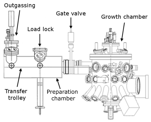
图1:。MBE系统原理示意图,显示加载锁定,传送系统,除气站和生长室请点击此处查看该图的放大版本。

III族氮化物可以在具有各种晶体取向衬底上生长。最常用的取向是镓极性的c面,它允许的二维电子气的形成而不掺杂通过利用阻挡层,通常AlGaN和GaN沟道之间偏振差。氮化镓的各种非极性和半极性方向已收到光电子显著注意由于在量子阱,这也使得这些取向不太希望为HEMT应用A 6,7-减小极化效应纳秒。 N极性导向设备是用于下一代高频HEMT操作有吸引力,由于比常规镓极性设备几个固有的优点。8在N极性装置的阻挡层生长在GaN沟道下方, 如图2,所得在自然回屏障有助于该信道的静电控制和减少短沟道效应,同时允许容易当前接入到GaN沟道和减少接触电阻。阻挡也可以从通道分别控制,这样,当信道厚度按比例缩小的用于高频器件的屏障设计可以被修改,以补偿失去的费米能级钉扎效应信道的费用。
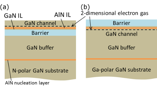
图2
2:(a)一种N极性HEMT和(b)一种镓极性HEMT为COMPAR的外延层概略层结构ISON。 请点击此处查看该图的放大版本。

在高速使用HEMT器件,高功率放大器通常生长在SiC衬底采取SiC的高热导率的优点。低的穿透位错密度的独立式GaN衬底可以被用来提高电子迁移率,9从而改善高频性能。以下的AlN成核层的生长,一个厚的GaN缓冲生长到空间中的杂质在离HEMT信道的再生长界面分离并改善电隔离。不像其他的III-V材料,氮化镓由PAMBE生长通常需要的生长条件与一组-III / V比大于1, ,富金属的条件下,10,11,以达到平滑的表面形态更大。 x中铝1×N是一个ALTER天然阻挡材料为III族氮化物HEMT器件,并已收到显著关注最近,因为它可以生长晶格匹配的GaN对于x≈0.18,并可以在相对的AlGaN障碍两次沟道电荷由于其高自发极化产生12-15不同于的AlGaN障碍,镓将优先结合到在InAlN层,16因而必须小心,以确保富Ga GaN缓冲层的生长和InAlN生长之前后的表面是自由过量的Ga。

镓的表面上控制可以通过suppling Ga的磁通比Ga的液滴形成所需的磁通稍小来完成。然而,这种增长窗口小,并且不足镓表面覆盖将导致表面形态降解成高原/沟槽的形态,而过量的Ga束流会导致镓积累和宏观液滴形成。17反射高能电子衍射(RHEED)INTENS性可用于监测镓积累和解吸。ガ表面覆盖率是通过RHEED强度降低,和关闭ガ之间任何滞后指示(和N *)百叶窗和在RHEED强度的初始增加表明镓累积, 如图3。

图3
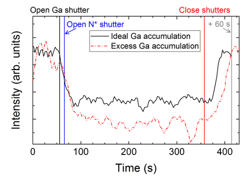
图3:监控嘎覆盖,使用触发采集下旋转收购RHEED模式计量的RHEED强度 RHEED强度信号 (未示出)不足Ga束流通过关闭快门之后立即增加强度指示。饱和/理想嘎覆盖率由快门关闭和突然的RHEED增白和多余嘎覆盖率视为初始RHEED增亮两个延迟以及导致全强度恢复较为缓慢强度增加的时间超过60秒之间的延迟表示。COM /文件/ ftp_upload / 54775 / 54775fig3large.jpg“目标=”_空白“>点击此处查看该图的放大版本。

实现高品质通过PAMBE InAlN由横向成分波动的存在复杂的,导致由以富以界包围富铝域的“蜂窝”的微观结构。此微结构18消除是通过使用基板温度约50取得℃下在解吸,15,19,20或约630℃,N极性InAlN发作以上。在这种高温下生长机制,则在具有In x Al 1-×N个组合物是衬底温度的强函数,以导致较低的掺入更高的温度。该通量可以增加以补偿蒸发掉,但实际上最大的在流量由掺入效率的降低与增加流量限制21除了降低衬底温度或增加在通量,增加生长速度也可以增加在组合物由于“以掩埋效应”,其中,进入的铝原子陷阱以及防止其蒸发。21,22高等生长速率可以通过按比例增加的In和Al通量来实现。为了保持生长条件Ñ富中,N *将需要以及增加,这可以通过增加RF等离子体功率来实现,增加 N 2流量,改善了等离子体室设计,或者增加光圈板孔密度。

在基于InAlN类HEMT额外外延层包括GaN和AlN中间层(离子液体)和GaN沟道。 AlN的IL插入的屏障和渠道之间能增加流动性μ以及沟道薄层电荷密度N s 。在移动性的增加归因于减少与InAlN B电子波函数重叠arrier和随后的合金散射。9为确保在AlN的IL高质量的增长,过量的Ga束流的生长过程中供给到充当表面活性剂。的GaN的IL可以在AlN IL和屏障之间使用,以进一步改善流动性,同时减少信道的费用。 GaN沟道可以在相同的温度下InAlN屏障来生长,允许从阻挡尽管离子液体和信道持续增长。改进的流动性已经被中断的AlN IL后生长和生长所述GaN沟道之前增加的生长温度下得到。在这种情况下的保护镓表面覆盖有中断,以防止流动性降解过程中被保持。

下面的协议特别适用于生长在N极性GaN衬底InAlN屏障HEMT器件。它可以通过包括一个50纳米厚的n富AlN层可以直接延伸到第C-极性4H-或6H-SiC衬底的生长。

Protocol

1.积液细胞斜坡和流量校准确认液态氮的流向低温板和生长室已达到基本压力。 斜坡上升的喷射室到其光束通量测量(BFM)温度以1℃/秒的升温速率为Ga和在细胞中,并为铝10℃/分钟。等待细胞1小时,热稳定。 打开每个单元的快门为30-60秒,然后关闭快门1-2分钟。重复三次每个小区。丢弃第一束流离子规测量和平均后两种。调整电池温度根据先前通量/温度校准以获得…

Representative Results

X射线衍射(XRD)上生长图4中N极性GaN衬底所示InAlN薄膜的扫描(a)的单峰值都为50和200纳米厚的薄膜。 50纳米厚的薄膜InAlN的XRD扫描表现Pendellösung条纹高达15 阶 ,显示非常高的界面质量。 图4中的非对称倒易空间映射(b)示出了200nm厚InAlN层具有相同q‖,因此在同一平面内晶格常数为GaN衬底,指示用于一?…

Discussion

高品质的GaN缓冲层的生长是在任何III族氮化物HEMT实现高电子迁移率的关键。在N极性InAlN HEMT的情况下,缓冲层生长是由所有镓从InAlN生长之前的表面去除的要求变得复杂。有各种技术,除了程序来完成此这里描述的,例如金属调制外延,27使用的生长条件在中间镓覆盖率和Ga液滴积累制度,28的边缘或允许连续N * -磁通掺入过量嘎当嘎快门被周期性关闭。24

<p class=…

Disclosures

The authors have nothing to disclose.

Acknowledgements

The authors thank Mr. Neil Green for assistance with sample preparation. This work was supported by the Office of Naval Research under funding from Dr. P. Maki. MTH was supported by a National Research Council Postdoctoral Fellowship.

Materials

Freestanding N-polar GaN wafer Kyma 10 mm x 10 mm
C-polar SiC wafer Cree W4TRE0R-L600 3 inch diameter
Microelectronics grade acetone Fischer Scientific A18-4
Microelectronics grade isoproponal J.T. Baker 9079-05/JT9079-5
Al source material (6N5 pure) UMC ALR62060I
Ga source material (7N pure) UMC GA701
In source material (7N pure) UMC IN750
ULSI N2 source gas (6N pure) Matheson Tri-gas G2659906D
PRO-75 MBE system OmicronScientia

References

  1. Hughes, W. C., et al. Molecular beam epitaxy growth and properties of GaN films on GaN/SiC substrates. J. Vac. Sci. Technol., B. 13 (4), 1571-1577 (1995).
  2. McSkimming, B. M., Wu, F., Huault, T., Chaix, C., Speck, J. S. Plasma assisted molecular beam epitaxy of GaN with growth rates 2.6 µm/hr. J. Cryst. Growth. 386, 168-174 (2014).
  3. Grandjean, N., Massies, J., Leroux, M. Nitridation of sapphire. Effect on the optical properties of GaN epitaxial overlayers. Appl. Phys. Lett. 69 (14), 2071-2073 (1996).
  4. Corrion, A. L., Wu, F., Speck, J. S. Growth regimes during homoepitaxial growth of GaN by ammonia molecular beam epitaxy. J. Appl. Phys. 112 (5), 054903 (2012).
  5. Mazumder, B., et al. Atom probe analysis of AlN interlayers in AlGaN/AlN/GaN heterostructures. Appl. Phys. Lett. 102 (11), 111603 (2013).
  6. Feezell, D. F., Speck, J. S., DenBaars, S. P., Nakamura, S. Semipolar (2021) InGaN/GaN Light-Emitting Diodes for High-Efficiency Solid State Lighting. J. Disp. Technol. 9 (4), (2013).
  7. Hardy, M. T., et al. True Green Semipolar InGaN-Based Laser Diodes Beyond Critical Thickness Limits Using Limited Area Epitaxy. J. Appl. Phys. 114 (18), 183101 (2013).
  8. Wong, M. H., et al. N-polar GaN epitaxy and high electron mobility transistors. Semicond. Sci. Technol. 28 (7), 074009 (2013).
  9. Hardy, M. T., et al. Charge control in N-polar InAlN high-electron-mobility transistors grown by plasma-assisted molecular beam epitaxy. J. Vac. Sci. Technol., B. 33 (6), 061207 (2015).
  10. Piquette, E. C., Bridger, P. M., Beach, R. A., McGill, T. C. Effect of Buffer Layer and III/V Ratio on the Surface Morphology of GaN Grown by MBE. Symposium G ‘-‘ GaN and Related Alloys. , (1998).
  11. Tarsa, E. J., et al. Homoepitaxial growth of GaN under Ga-stable and N-stable conditions by plasma-assisted molecular beam epitaxy. J. Appl. Phys. 82 (11), 5472-5479 (1997).
  12. Kuzmik, J. Power electronics on InAlN/(In)GaN: Prospect for a record performance. IEEE Electron Device Lett. 22 (11), 510-512 (2001).
  13. Fernández-Garrido, S., Gačević, &. #. 3. 8. 1. ;., Calleja, E. A comprehensive diagram to grow InAlN alloys by plasma-assisted molecular beam epitaxy. Appl. Phys. Lett. 93 (19), 191907 (2008).
  14. Katzer, D. S., et al. Molecular beam epitaxy of InAlN∕GaN heterostructures for high electron mobility transistors. J. Vac. Sci. Technol., B. 23 (3), 1204-1208 (2005).
  15. Kaun, S. W., et al. GaN-based high-electron-mobility transistor structures with homogeneous lattice-matched InAlN barriers grown by plasma-assisted molecular beam epitaxy. Semicond. Sci. Technol. 29 (4), 045011 (2014).
  16. Hoke, W. E., Torabi, A., Mosca, J. J., Kennedy, T. D. Thermodynamic analysis of cation incorporation during molecular beam epitaxy of nitride films using metal-rich growth conditions. J. Vac. Sci. Technol., B. 25 (3), 978-982 (2007).
  17. Koblmüller, G., Reurings, F., Tuomisto, F., Speck, J. S. Influence of Ga/N ratio on morphology, vacancies, and electrical transport in GaN grown by molecular beam epitaxy at high temperature. Appl. Phys. Lett. 97 (19), 191915 (2010).
  18. Zhou, L., Smith, D. J., McCartney, M. R., Katzer, D. S., Storm, D. F. Observation of vertical honeycomb structure in InAlN∕GaN heterostructures due to lateral phase separation. Appl. Phys. Lett. 90 (8), 081917 (2007).
  19. Ahmadi, E., et al. Elimination of columnar microstructure in N-face InAlN, lattice-matched to GaN, grown by plasma-assisted molecular beam epitaxy in the N-rich regime. Appl. Phys. Lett. 104 (7), 072107 (2014).
  20. Hardy, M. T., et al. Morphological and microstructural stability of N-polar InAlN thin films grown on free-standing GaN substrates by molecular beam epitaxy. J. Vac. Sci. Technol., A. 34 (2), 021512 (2016).
  21. Hardy, M. T., et al. Indium incorporation dynamics in N-polar InAlN thin films grown by plasma-assisted molecular beam epitaxy on freestanding GaN substrates. J. Cryst. Growth. 245, (2015).
  22. Leszczynski, M., et al. Indium incorporation into InGaN and InAlN layers grown by metalorganic vapor phase epitaxy. J. Cryst. Growth. 318 (1), 496-499 (2011).
  23. Storm, D. F., et al. Ultrathin-barrier AlN/GaN heterostructures grown by rf plasma-assisted molecular beam epitaxy on freestanding GaN substrates. J. Cryst. Growth. 380, 14-17 (2013).
  24. Storm, D. F., Katzer, D. S., Meyer, D. J., Binari, S. C. Oxygen incorporation in homoepitaxial N-polar GaN grown by radio frequency-plasma assisted molecular beam epitaxy: Mitigation and modeling. J. Appl. Phys. 112 (1), 013507 (2012).
  25. Storm, D. F., et al. Effect of interfacial oxygen on the microstructure of MBE-grown homoepitaxial N-polar. J. Cryst. Growth. 409, 14 (2014).
  26. Meyer, D. J., et al. High Electron Velocity Submicrometer AlN/GaN MOS-HEMTs on Freestanding GaN Substrates. IEEE Electron Device Lett. 34, 199 (2013).
  27. Moseley, M., Billingsley, D., Henderson, W., Trybus, E., Doolittle, W. A. Transient atomic behavior and surface kinetics of GaN. J. Appl. Phys. 106 (1), 014905 (2009).
  28. Koblmüller, G., et al. Ga Adlayer Governed Surface Defect Evolution of (0001)GaN Films Grown by Plasma-Assisted Molecular Beam Epitaxy. Jpn. J. Appl. Phys. 44 (28), L906-L908 (2005).
  29. Poblenz, C., Waltereit, P., Speck, J. S. Uniformity and control of surface morphology during growth of GaN by molecular beam epitaxy. J. Vac. Sci. Technol., B. 23 (4), 1379-1385 (2005).
check_url/kr/54775?article_type=t

Play Video

Cite This Article
Hardy, M. T., Storm, D. F., Katzer, D. S., Downey, B. P., Nepal, N., Meyer, D. J. Plasma-assisted Molecular Beam Epitaxy of N-polar InAlN-barrier High-electron-mobility Transistors. J. Vis. Exp. (117), e54775, doi:10.3791/54775 (2016).

View Video