- 00:06Overview
- 00:58Principles of Boost Converters
- 05:01Board Setup
- 07:12Boost Converter Testing with Variable Input
- 08:38Boost Converter Testing with Variable Duty Ratio
- 09:53Results
- 11:02Applications
- 11:56Summary
ממיר האצת DC/DC
English
Share
Overview
מקור: עלי באזי, המחלקה להנדסת חשמל, אוניברסיטת קונטיקט, סטורים, CT.
ממירי Boost מספקים פתרון רב-תכליתי להגברת מתחי DC ביישומים רבים שבהם יש להגדיל מתח DC ללא צורך להמיר אותו ל- AC, באמצעות שנאי ולאחר מכן לתקן את יציאת השנאי. ממירי Boost הם ממירי מדרגה המשתמשים בגרם כהתקן אחסון אנרגיה התומך בפלט עם אנרגיה נוספת בנוסף למקור הקלט DC. זה גורם למתח היציאה להגביר.
מטרת הניסוי הזה היא לחקור מאפיינים שונים של ממיר דחיפה. יכולת השלב של הממיר תיצפה במצב הולכה רציף (CCM) שבו זרם המשרן אינו אפס. ייעשה שימוש בפעולת לולאה פתוחה עם יחס חובה קבוע באופן ידני. הערכה של יחסי הקלט-פלט תיבחן.
Principles
ממיר האצה מסתמך על אנרגיה המאוחסנת במשרן, L, כדי לספק אנרגיה לצד הפלט שבו העומס נתמך, בנוסף למקור DC להיות מקור האנרגיה העיקרי. הרעיון העיקרי מאחורי פעולת ממיר דחיפה הוא כי משרן יהיה להפוך את קוטביות המתח שלה כדי לשמור על זרימת הזרם. כפי שמוצג ב Fig. 1(a) עבור מעגל ממיר דחיפה פשוטה, כאשר המתג מופעל עבור מחזור חובה D של תקופת המיתוג T, מתח משרן VL מצטבר. כאשר המתג כבוי, זרם המשרן צריך להמשיך לזרום ולכן קוטביות המתח של המשרן תתהפך כדי להוסיף למתח הכניסה Vב-.
עם זאת, כאשר המתג מופעל, העומס קצר ומתח היציאה הוא אפס, אשר אינו רצוי. לכן, דיודה חוסמת מתווספת בצד הפלט כפי שמוצג ב- Fig. 1(b) כדי למנוע קצר בעומס. דיודה זו עדיין אינה פותרת את בעיית העומס ואינה רואה מתח כאשר המתג מופעל, ולכן קבל נוסף כפי שמוצג ב- Fig. 1(c) כדי לספק לעומס את הזרם הדרוש במהלך התקופה שבה המתג מופעל. שים לב שכאשר המתג מופעל, הדיודה כבויה (מוטה לאחור) ולהיפך. מתח היציאה הממוצע קשור אפוא למתח הכניסה כמו: <Vהחוצה> = Vב/ (1-D).
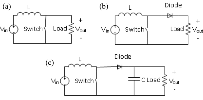
איור 1. שלבים לבניית ממיר האצה
ככל שניסוי זה מתקדם, יוצגו כי מתח היציאה הממוצע עולה ככל שמחזור החובה, D, גדל. זה נכון שכן מתח היציאה ליחסי מתח הכניסה הוא יחסי הפוך ל-D, ולכן מתח היציאה ו- D יש מתאם חיובי.
שים לב שהמשוואה המוצגת היא עבור ממיר האצה אידיאלי, ועשויה להיראות כאילו D = 1 יניב מתח יציאה אינסופי, אך זה לא נכון. במציאות, אלמנטים טפשיים והתנגדות בממיר דחיפה לגרום D להיות מוגבל סביב 70-80% ולאחר מכן השפעות טפשיות להתחיל לשלוט על פעולת המעגל ולגרום ירידות מתח משמעותיות. בשלב כזה, מתח היציאה מתחיל לרדת ככל ש- D עולה. עם תדרי מיתוג גבוהים יותר, אדווה המתח בפלט תקטן מכיוון שזמן הטעינה והפירוק של המתח הקבלי יתקצר משמעותית עם ירידה בתדר המיתוג.
Procedure
Results
The boost converter output-input voltage relationship is proportional to the duty cycle in the sense that higher D will yield higher output voltages for a given input voltage. If the input voltage is Vinand the output voltage is Vout, Vout/Vin= 1/(1-D), where 0≤D≤ 100%. Therefore, for an input voltage of 10 V, Vout≈ 12.5 V for D = 20%, Vout≈ 16.67 V for D= 40%, and Vout≈ 25 V for D = 60%.
Nevertheless, the output voltage will be lower than expected from the ideal relationship, which is linear with the duty ratio. The main reason is that the ideal converter model from which the Vout/Vin relationship can be derived does not account for non-idealities and voltage drops in the converter. Theoretically, as D→100%, Vout→∞; practically, a theoretical limit on the boosting capability is around 3-4x the input voltage, and after a certain level of D, the output voltage of the converter starts to drop rather than being boosted due to parasitic and non-ideal elements in a real converter.
Applications and Summary
Boost converters are very common in solar photovoltaic applications where the input voltage from the solar panel varies with weather conditions and available solar energy, and a boost converter can always boost from the PV panel voltage. Power factor correction to improve power quality as seen from the utility grid with power electronic loads which may require significant reactive power, e.g. motors, is another major application of boost converters.
Transcript
Boost converters are used in electronics to generate a DC output voltage that is greater than the DC input, therefore boosting up the supply voltage. Boost converters are often used in power supplies for white LEDs, battery packs for electric automobiles, and many other applications. A boost converter stores energy in an inductor’s magnetic field and transfers it to a load with a switching circuit. The transfer of energy from the inductor’s magnetic field enables the increase in DC output in a single stage. This video will illustrate the construction of a boost converter and investigate how changing the converter’s operating condition affects its output voltage.
This simple boost converter circuit consists of an input DC voltage source connected to an inductor and a switch. The switch may be a bipolar transistor, a MOSFET or, other similar electronic device that alternately connects and disconnects the inductor from the common line of the power supply. A blocking diode connects the inductor to a capacitor which filters the ripple in the output voltage. Increasing the capacitance decreases the ripple. For a sufficiently large capacitance the output becomes a steady DC voltage. A digital pulse train opens or closes the switch. The pulse has a duty ratio which is the ratio of the on time to the period. The duty ratio may vary from zero or increase up to one with more and more on time. When the pulse is on, the switch closes and the inductor is connected across the supply voltage. In this state, the inductor terminal connected to the output of the power supply has the higher potential and the terminal connected to the common has the lower potential. Now current flows through the inductor increasing linearly with time for sufficiently high switching frequencies. During this time the inductor voltage is defined to be positive because the slope of the current versus time is positive. The inductor stores energy proportional to the square of the current in its magnetic field. The longer the inductor is connected to the power supply, the more current increases and the more energy it stores. When the switch opens, current through the inductor must continue flowing in the same direction. This current also decreases because the inductor now gives up energy to the load. The inductor voltage becomes negative because the slope of current versus time is negative. As a result, the inductor’s polarity flips and now adds to input voltage “V in” producing a higher potential at the output. The circuit in this state, forward biases the diode and the inductor discharges current, some going to the load, and some going to the capacitor which then stores the charge. When the switch closes again the diode becomes reverse biased disconnecting the inductor from the output and preventing a short circuit of the load. During this time the inductor recharges and in its place the capacitor provides current to the load. This cycle of capacitor charging and discharging produces an average output voltage with some amount of ripple. At sufficiently high switching frequencies, the capacitor’s charge and discharge times are short and the output reaches a steady state voltage with relatively little ripple. This switching cycle repeats indefinitely and is the basis of boost converter operation. Ideally the average output voltage increases as the duty ratio increases and a duty ratio of one generates infinite voltage. However parasitic elements and resistances in the boost converter limit useful values of D to a maximum of about 0.7 or 0.8. If D is sufficiently large, parasitic effects dominate circuit operation and output voltage decreases even as D continues to increase. In the following experiments we will study how a boost converter steps up voltage in continuous conduction mode, also called CCM, a condition when the inductor operates at all times with non zero current.
The output voltage in this experiment is limited to 50 volts DC or less. Use only the specified duty cycles, frequencies, input voltages, and loads. These experiments utilize the HiRel Systems Power Pole Board which is designed for experimentation with different DC to DC converter circuit topologies. With signal supply switch S90 turned off, plug the +/- 12 volt signal supply into den connector J90. Set the PWM control selection jumpers J62 and J63 to the open loop position. Adjust the DC power supply to positive 10 volts but do not connect the power supply output to the board. Next build the circuit as shown with the lower MOSFET, the upper diode, and the BB magnetic board. Record the value of the inductor on the BB magnetic board. The load resistor is a power potentiometer. Use a multi meter to measure it’s resistance while adjusting it to 20 ohms. Then connect the potentiometer between terminals V1+ and COM. Set switch selector bank S30 as follows: PWM to bottom MOSFET, use onboard PWM, and switched load off. Connect the oscilloscope’s differential probe between terminal 16 which is the gate of the lower MOSFET and terminal 12 which is the source. Turn on switch S90. The pulse train that drives the MOSFET should appear on the scope’s screen. Select the scope’s time axis to display several periods of this wave form. Set frequency adjustment potentiometer RV60 to produce a switching frequency of 100 kilohertz. Set duty ratio potentiometer RV64 so the pulses have an on time of one microsecond which corresponds to a duty ratio of 0.1.
Connect the DC power supply to input terminals V2+ and COM. To measure the inductor current connect the differential scope probe between terminals CS5 and COM. To measure the voltage across load resistor RL, connect the other differential probe between terminals V1+ and COM. The output voltage should be a triangle wave. The upward ramps occur when the boost convertor switch is open and the inductor is transferring energy to the load. The downward ramps occur when the switch is closed, the inductor is disconnected from the output, and the capacitor is supplying energy to the load. The inductor current is a triangle wave which ramps up linearly during the on time of the pulse train, then ramps down linearly during the off time. The offset is the average current. Using the scope’s built in measurement functions, measure the mean value of the output voltage and the mean value of the inductor current. Repeat these steps with the input DC power supply set to eight, 12, and 14 volts. For a fixed duty ratio as the input voltage increases the output voltage of an ideal boost converter should increase proportionally.
This part of the experiment measures the duty ratio of the pulse train instead of the inductor current. Connect the scope probes between terminals 16 and 12 which are the gate and source of the lower MOSFET respectively. Connect the input DC power supply to terminals V2+ and COM. Like before, the output voltage is a triangle wave resulting from the inductor and capacitor alternately supplying current to the load. The gate source voltage of the MOSFET is a digital pulse train with a frequency of 100 kilohertz, a period of 10 microseconds, and an on time of one microsecond. Measure the mean value of the output voltage and the on time of the gate to source voltage along with the input current and voltage readings from the DC power supply. Repeat this test after adjusting duty ratio potentiometer RV64 so the pulse stream has an on time of two, four, and six microseconds, which correspond to duty ratios of 0.2, 0.4, and 0.6 respectively.
As duty ratio D increases, the output voltage of the boost converter also increases. Ideally if D has a value of 0.2 then an input of 10 volts generates an output of about 12.5 volts. If D is 0.4 then the output would be about 16.6 volts. If D is 0.6 then the output would be about 25 volts. In general, the output voltage is less than expected from the ideal relationship because parasitic elements create non ideal voltage drops and unaccounted energy loss. As the duty ratio approaches one, the theoretical output voltage becomes infinitely large. In reality, the output voltage is limited to about three or four times the input voltage and the influence of parasitic and non ideal components causes the output voltage to decrease after D becomes sufficiently high.
Boost converters generate an output voltage that is greater than the input voltage and many applications incorporate them to increase flexibility in the choice of power sources. The voltage from a solar panel changes with the position of the sun, weather conditions, and shade. Boost converters are commonly used to step up the variable output of a solar panel array to provide a consistent voltage to feed into an electrical grid. Battery powered systems are frequently used to power devices without the use of a power cord. In order to achieve the necessary higher output voltage, battery cells are often stacked. This can take up a lot of space if many cells are needed to reach the desired output. Instead, boost converters are used to step up the voltage while conserving space.
You have just watched Jove’s Introduction to Boost Converters. You should now understand how boost converters work and how adjusting input voltage, duty ratio, and frequency affects the output voltage. Thanks for watching.