X射线光电子光谱
English
Share
Overview
资料来源:佐治亚州佐治亚州理工学院材料科学与工程学院费萨尔·阿拉姆吉尔,佐治亚州亚特兰大
X射线光电子光谱(XPS)是一种测量材料中元素元素成分、经验公式、化学状态和电子状态的技术。XPS光谱是通过用X射线束照射材料获得,同时测量从被分析材料顶部几纳米中逸出的动能和电子数量(在 = 前 10 nm 内,用于典型动力学电子的能量)。由于信号电子主要从材料的前几纳米内逃逸,XPS被认为是一种表面分析技术。
XPS背后的物理原理的发现和应用,或者正如前面所知,用于化学分析的电子光谱学(ESCA),导致了两项诺贝尔物理学奖。第一次于1921年授予阿尔伯特·爱因斯坦,因为他在1905年解释了光电效应。光电效应是XPS中产生信号过程的基础。不久之后,凯·西格巴恩根据因内斯、莫斯利、罗林森和罗宾逊的早期作品开发了ESCA,并在1954年记录了NaCl的第一个高能分辨率XPS频谱。ESCA/XPS在化学分析方面的力量的进一步展示,以及该技术相关仪器的开发,导致1969年第一个商业单色XPS仪器和1981年诺贝尔物理学奖授予Siegbahn,以表彰他为开发该技术作为分析工具而作出的广泛努力。
Principles
Procedure
Results
Figure 1 shows a survey spectrum from the sample, clearly showing the Pt, Si, C and O emissions. In Figure 2, we see the high resolution scan of the Pt 4f7/2 and 4f5/2 peaks from the sample. The binding energies of each of the core level peaks can be compared to those found in databases such as the one maintained by the National Institute of Standards and Technology (NIST) (at https://srdata.nist.gov/xps/Default.aspx). The subtle shifts in binding energy relative to those of the reference compounds in the database can reveal the chemical state of each of the elements in your sample. The intensity ratio of the peaks will reveal the surface composition.
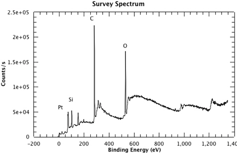
Figure 1: A survey spectrum from the sample, clearly showing the Pt, Si, C and O emissions.
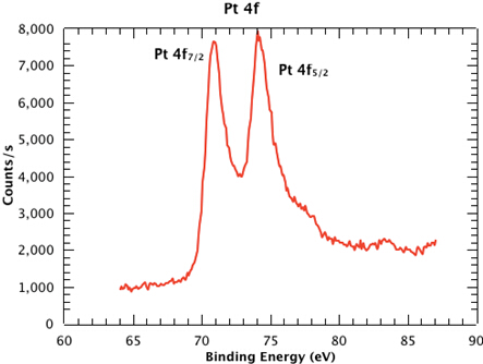
Figure 2: High resolution scan of the Pt 4f7/2 and 4f5/2 peaks from the sample.
Applications and Summary
XPS is a surface chemical analysis technique that is versatile in the range of samples it can be used to investigate. The technique provides quantification of chemical composition, chemical state and the occupied electronic structure of the atoms within a material.
XPS provides elemental the composition of the surface (within 1-10 nm usually), and can be used to determine the empirical formula of the surface compounds, the identity of elements that contaminate a surface, the chemical or electronic state of each element in the surface, the uniformity of composition across top surface and through the depth (by sequentially milling into the material and taking XPS data of the new exposed surface).
Routinely, XPS is used to analyze a wide range of materials, for example metal alloys, other inorganic compounds such as ceramics, polymers, semiconductors, catalysts, glasses, parts of plants biological materials such as cells, bones and many others.
Transcript
X-ray photoelectron spectroscopy, or XPS, is an non-destructive technique that can be used to measure the surface chemistry of a material. In XPS, an X-ray of known energy strikes an atom. A core shell electron absorbs the X-ray photon, gaining enough energy to leave its orbit.
Excess energy absorbed by the electron remains as its kinetic energy. By assembling a spectrum of these kinetic energies, the original binding energies of the electrons can be calculated and used to determine the chemical composition and state of the material.
This video will explain the principles of X-ray photoelectron spectroscopy and will demonstrate how to measure and interpret an XPS spectrum.
When a bound electron absorbs a photon of sufficient energy, it is ejected from its orbit. For a tightly bound core shell electron to be ejected, it must absorb a highly energetic X-ray photon. If the absorbed photon carries enough additional energy to exceed the threshold work function of the material, the electron may escape into the vacuum. These electrons are referred to as photoelectrons. Any remaining energy from the X-ray appears as the kinetic energy of the photoelectron.
For X-ray photoelectron spectroscopy, X-ray sources of known energy are used. One common source is aluminum K alpha, which produces 1,486.7 electron volt X-rays. The X-ray’s energy and the work function of the surface are used in conjunction with the measured kinetic energy of the photoelectron to determine the electron’s original binding energy. The binding energy is equal to the original energy of the X-ray source, minus the work function energy of the surface and the remnant kinetic energy of the photoelectron. Once a spectrum has been collected, energy peaks can be compared with those of reference samples.
Subtle shifts in the energy of the measured peaks from reference peaks, as well as the relative heights between peaks of the measured spectrum, can be used to determine the elemental composition, chemical states, and electronic states of elements in the sample. XPS is useful to a depth of approximately 10 nanometers.
Now that you understand the principles behind XPS, you are now ready to measure a spectrum.
It is important to follow cleanliness rules for ultra-high vacuum systems when measuring an X-ray photoelectron spectrum. Polyethylene or powder-free nitrile gloves should be worn. And tweezers should be used to handle the sample slide. The sample should be stored in a glass container, which is then covered, so that they may be transported safely to the X-ray photoelectron spectrometer. Note that the following procedure applies to a specific XPS instrument and its associated software, and there may be some variations when other instruments are used.
In order to load the samples, first vent the load-lock chamber to access the sample holder. This should take several minutes. When the chamber has vented to atmospheric pressure, the door will spring open. Once the load-lock chamber opens, remove the sample holder from the transfer arm. To prevent contamination from previous analyses, clean the sample holder thoroughly by wiping it down with isopropyl alcohol. Be sure to clean the metal clip as well. Load each slide into the sample holder by pressing it under the metal clips.
Then return the sample holder to the load-lock chamber and place it on the transfer arm. When the sample holder is seated properly, close the chamber door. Pump down the load-lock chamber until the pressure registers in the 10 to the minus seven millibar range. This should take several minutes. Some samples, such as powders, highly porous materials, or those containing unevaporated solvents may take longer.
Finally, transfer the samples to the analysis chamber. When the chamber pressure is in the 10 to the minus eight millibar range, you can begin to collect a spectrum.
Now that the samples have been loaded and are ready to be analyzed, set the pass energy for the spectrometer. The pass energy is the energy with which all photoelectrons will enter the spectrometer. The pass energy sets a constant resolution for the entire spectrum. Setting a high pass energy results in a higher flux of photoelectrons and a greater signal to noise ratio for the experiment, but a worse resolution.
A spectrum taken with a low pass energy setting has a better resolution, but a lower signal to noise ratio. Now that the pass energy has been set, the next task is to collect a survey spectrum of our sample. The survey spectrum covers a broad range of energies in order to include all of the various types of electrons ejected from the surface. This spectrum will allow for the inspection of all photoelectron emission peaks prior to choosing a specific energy region to scan.
For this survey spectrum, the sample is a thin layer of platinum grown on a single layer of graphene, which is supported by a commercial silica glass slide. Peaks corresponding to platinum, silicon, carbon, and oxygen can be seen in the spectrum. The silicon and carbon peaks arise from the media supporting the sample. The oxygen peak is a result of water in the atmosphere adhering to the surface. The platinum peaks appear between 60 and 90 electron volts. These are the peaks we are interested in. Now that a survey spectrum has been collected, and a region of interest has been determined, we can collect a high resolution XPS spectrum.
Measuring a spectrum typically takes between 30 minutes and an hour for a set that includes a survey and a few different high resolution regions. When the spectrum is complete, the results are ready to be analyzed.
Now that a high resolution XPS spectrum has been produced, the peaks can be compared to the core level binding energy peaks found in reference databases.
Subtle shifts in binding energies relative to those of the reference compounds indicate the chemical state of each of the elements in the sample. The intensity ratio between peaks of the spectrum reveals the surface composition.
XPS is used routinely to analyze a wide range of materials such as metal alloys, ceramics, polymers, semiconductors, and biological materials. XPS is an important tool for characterizing the surfaces of thin, semiconductor films used to produce microelectronics. Precisely determining the surface chemistry aids in the detection of contaminants, which can improve the manufacturing process.
In addition, XPS enables researchers to relate novel properties of a particular semiconductor to its chemistry, which is critical to the development of new materials. XPS can also be used to analyze biological samples such as fossilized bone. The chemical makeup of fossil remains carries a great deal of information. Using XPS, we can learn about the biology of evolution of the organisms, their environment, and the conditions under which they were fossilized.
You’ve just watched Jove’s introduction to X-ray photoelectron spectroscopy. You should now understand the principles behind XPS, how to collect an XPS spectrum, and how to interpret the results to determine the composition and state of a sample material.
Thanks for watching.