Summary

金属辅助多孔硅和固体硅晶圆的电化学纳米压印

Published: February 08, 2022
doi:

Summary

提出了一种金属辅助化学印迹的方案,将形状精度低于20 nm的3D微尺度特征印制到固体和多孔硅晶圆中。

Abstract

金属辅助电化学压印(Mac-Imprint)是金属辅助化学蚀刻(MACE)和纳米压印光刻的组合,能够直接图案化单晶IV族(例如Si)和III-V(例如GaAs)半导体中的3D微米和纳米级特征,而无需牺牲模板和光刻步骤。在此过程中,在氢氟酸(HF)和过氧化氢(H2O2)混合物存在的情况下,涂有贵金属催化剂的可重复使用的印章与Si晶圆接触,这导致Si在金属 – 半导体接触界面处选择性蚀刻。在该协议中,我们讨论了在两种Mac-压印配置中应用的印章和底物制备方法:(1)具有固体催化剂的多孔Si Mac压印;(2)固体Si Mac-压印与多孔催化剂。该过程具有高通量,能够以低于20nm的分辨率进行厘米级的平行图案化。它还可在单次操作中提供低缺陷密度和大面积图案化,并绕过了深度反应离子蚀刻(DRIE)等干法蚀刻的需要。

Introduction

半导体的三维微米和纳米级图案化和纹理化在各个领域具有众多应用,例如光电子学12,光子学3,抗反射表面4,超疏水和自清洁表面56 等。通过软光刻和纳米压印光刻,以低于20nm的分辨率成功完成了聚合物薄膜的原型设计和批量生产3D和分层图案。然而,将这种3D聚合物图案转移到Si中需要在反应离子蚀刻过程中掩模图案的蚀刻选择性,从而限制了纵横比,并且由于扇形效应而导致形状变形和表面粗糙度78

一种称为Mac-Imprint的新方法已经实现,用于多孔9和固体Si晶圆1011以及固体GaAs晶圆的平行和直接图案化121314。Mac-Imprint是一种基于接触的湿法蚀刻技术,要求基板与贵金属涂层印章在存在由HF和氧化剂(例如,Si Mac-压印的情况下为H2O2)组成的蚀刻溶液(ES)的情况下具有3D特征的接触。在蚀刻过程中,两种反应同时发生1516:阴极反应(即贵金属处的H2O2还原,在此期间产生正电荷载体[孔]并随后注入Si17)和阳极反应(即Si溶解,在此期间消耗空穴)。经过足够的时间接触后,印章的3D特征被蚀刻到硅晶圆中。与传统的光刻方法相比,Mac-Imprint具有许多优点,例如高通量,与卷对板和卷对卷平台,无定形,单晶和多晶硅和III-V半导体的兼容性。Mac-Imprint 邮票可以重复使用多次。此外,该方法可以提供低于20 nm的蚀刻分辨率,与当代直接书写方法兼容。

实现高保真压印的关键是到蚀刻前端的扩散途径(即催化剂和基板之间的接触界面)。Azeredo等人的工作 首先证明了ES扩散是通过多孔Si网络实现的。Torralba等人报道说,为了实现固体Si Mac-压印,ES扩散是通过多孔催化剂实现的。Bastide et al.19 和 Sharstniou et al.20 进一步研究了催化剂孔隙度对 ES 扩散的影响。因此,Mac-Imprint的概念已经在三种具有不同扩散途径的配置中进行了测试。

在第一种结构中,催化剂和基板是固体的,不提供初始扩散途径。缺乏反应物扩散导致在压印过程中发生二次反应,在催化剂-Si界面边缘周围的基板上形成一层多孔Si。反应物随后耗尽,反应停止,导致印章和底物之间没有可辨别的图案转移保真度。在第二种和第三种配置中,扩散途径通过引入基底(即多孔Si)或催化剂(即多孔金)中的多孔网络来实现,并且实现了高图案转移精度。因此,通过多孔材料的质量传递在使反应物和反应产物扩散到接触界面和远离接触界面9181920方面起着关键作用。所有三种配置的原理图如图1所示。

Figure 1
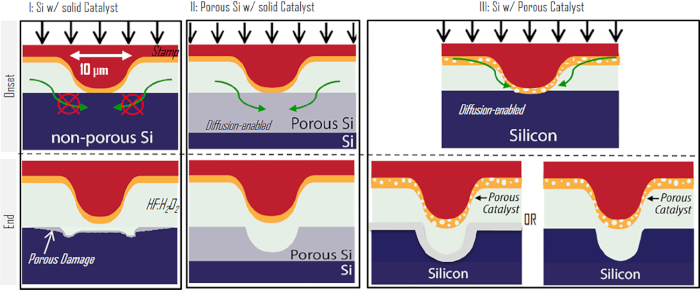
图 1:Mac-Imprint 配置示意图。 该图突出了多孔材料在使反应物质通过基体(即,情况II:多孔硅)或印章(即情况III:由多孔金制成的催化剂薄膜)扩散方面的作用。 请点击此处查看此图的放大版本。

在本文中,对Mac-Imprint工艺进行了深入讨论,包括印章准备和基材预处理以及Mac-Imprint本身。协议中的衬底预处理部分包括硅晶圆清洗和硅晶圆图案化,包括干蚀刻和衬底阳极氧化(可选)。此外,将印章准备部分细分为几个程序:1)Si主模具的PDMS复制成型;2)光刻胶层的紫外纳米压印,以转移PDMS图案;3)通过磁控溅射进行催化层沉积,然后进行脱合金(可选)。最后,在Mac-Imprint部分中,介绍了Mac-Imprint设置以及Mac-Imprint结果(即Si表面3D分层图案)。

Protocol

注意:使用适当的安全措施和个人防护装备(例如,实验室外套、手套、安全眼镜、露趾鞋)。该程序使用HF酸(48%重量),这是一种极其危险的化学物质,需要额外的个人防护装备(即面罩,天然橡胶围裙和第二副覆盖手,手腕和前臂的丁腈手套)。 1. 印章准备 PDMS模具制造 通过将去离子纯(DI)水和氢氧化铵以5:1的比例(体积)混合在玻璃烧…

Representative Results

为了研究Mac-Imprint邮票和印迹Si表面的形态特性,获得了扫描电子显微镜(SEM)图像,光学显微镜扫描(图9)和原子力显微镜(AFM)扫描(图10)。将压印固体Si的横截面轮廓与所用多孔金印章的横截面轮廓进行比较(图10)。在Mac-Imprint过程中,图案转移保真度和多孔Si生成是分析实验成功的两个主要标准?…

Discussion

分别根据协议的第1节和第2节制作了Mac印记印章和预图案硅芯片(p型,[100]方向,1-10欧姆∙cm)。根据协议的第3节执行带有包含3D分层图案的邮票的预图案Si芯片的Mac-Imprint(图9)。如图9a所示,应用了Mac-Imprint的不同构型:固体硅与固体金(左),多孔硅与固体金(中间)9,固体硅与多孔金(右)20。在…

Divulgations

The authors have nothing to disclose.

Acknowledgements

我们感谢Keng Hsu博士(路易斯维尔大学)对这项工作的见解;伊利诺伊大学弗雷德里克·塞茨实验室(Frederick Seitz Laboratory)和工作人员斯科特·麦克拉伦(Scott Maclaren)在纪念中;亚利桑那州立大学LeRoy Eyring固态科学中心;和比斯格罗夫学者奖下的亚利桑那州科学基金会。

Materials

Acetone, >99.5%, ACS reagent Sigma-Aldrich 67-64-1 CAUTION, chemical
Ammonium fluoride, >98%, ACS grade Sigma-Aldrich 12125-01-8 CAUTION, hazardous
Ammonium hydroxide solution, 28-30%, ACS reagent Sigma-Aldrich 1336-21-6 CAUTION, hazardous
AZ 400K developer Microchemicals AZ 400K CAUTION, chemical
BenchMark 800 Etch Axic BenchMark 800 Reactive ion etching
Chromium target, 2" x 0.125", 99.95% purity ACI alloys ADM0913 Magnetron sputter chromium target
CTF 12 Carbolite Gero C12075-700-208SN Tube furnace
Desiccator Fisher scientific Chemglass life sciences CG122611 Desiccator
F6T5/BLB Eiko F6T5/BLB 6W UV bulb
Gold target, 2" x 0.125", 99.99% purity ACI alloys N/A Magnetron sputter gold target
Hotplate KW-4AH Chemat tecnologie KW-4AH Leveled hotplate with uniform temperature profile
Hydrofluoric acid, 48%, ACS reagent Sigma-Aldrich 7664-39-3 CAUTION, extremly hazardous
Hydrogen peroxide, 30%, ACS reagent Fisher Chemical 7722-84-1 CAUTION, hazardous
Isopropyl alcohol, >99.5%, ACS reagent LabChem 67-63-0 CAUTION, chemical
MLP-50 Transducer Techniques MLP-50 Load cell
Nitric acid, 70%, ACS grade SAFC 7697-37-2 CAUTION, hazardous
NSC-3000 Nano-master NSC-3000 Magnetron sputter
Potassium hydroxide, 45%, Certified Fisher Chemical 1310-58-3 CAUTION, chemical
Rocker 800 vacuum pump, 110V/60Hz Rocker 1240043 Oil-free vacuum pump
Silicon master mold NILT SMLA_V1 Silicon chip with pattern
Silicon wafers, prime grade University wafer 783 Si wafer
Silver target, 2" x 0.125", 99.99% purity ACI alloys HER2318 Magnetron sputter silver target
SP-300 BioLogic SP-300 Potentiostat
SPIN 150i Spincoating SPIN 150i Spin coater
SPR 200-7.0 positive photoresist Microchem SPR 220-7.0 CAUTION, chemical
Stirring hotplate Thermo scientific Cimarec+ SP88857100 General purpose hotplate
SU-8 2015 negative photoresist Microchem SU-8 2015 CAUTION, chemical
SYLGARD 184 Silicone elastomere kit DOW 4019862 CAUTION, chemical
T-LSR150B Zaber Technologies T-LSR150B-KT04U Motorized linear stage
Trichloro(1H,1H,2H,2H-perfluorooctyl)silane (PFOCS), 97% Sigma-Aldrich 78560-45-9 CAUTION, hazardous

References

  1. Ning, H., et al. Transfer-Printing of Tunable Porous Silicon Microcavities with Embedded Emitters. ACS Photonics. 1 (11), 1144-1150 (2014).
  2. Hirschman, K. D., Tsybeskov, L., Duttagupta, S. P., Fauchet, P. M. Silicon-based light emitting devices integrated into microelectronic circuits. Nature. 384, 338-341 (1996).
  3. Cho, J., et al. Nanoscale Origami for 3D Optics. Small. 7 (14), 1943-1948 (2011).
  4. Azeredo, B. P., et al. Silicon nanowires with controlled sidewall profile and roughness fabricated by thin-film dewetting and metal-assisted chemical etching. Nanotechnology. 24 (22), 225305-225312 (2013).
  5. Lin, C., Tsai, M., Wei, W., Lai, K., He, J. Packaging Glass with a Hierarchically Nanostructured Surface: a universal method to achieve selfcleaning omnidirectional solar cells. ACS Nano. 10 (1), 549-555 (2016).
  6. Park, K. C., et al. Nanotextured Silica Surfaces with Robust Superhydrophobicity and Omnidirectional Broadband Supertransmissivity. ACS Nano. 6 (5), 3789-3799 (2012).
  7. Kim, J., Joy, D. C., Lee, S. Controlling resist thickness and etch depth for fabrication of 3D structures in electron-beam grayscale lithography. Microelectronics Engineering. 84 (12), 2859-2864 (2007).
  8. Deng, S., Zhang, Y., Jiang, S., Lu, M. Fabrication of three-dimensional silicon structure with smooth curved surfaces. Journal of Micro/Nanolithography, MEMS, and MOEMS. 15 (3), 0345031-0345036 (2016).
  9. Azeredo, B. P., Lin, Y., Avagyan, A., Sivaguru, M., Hsu, K. Direct Imprinting of Porous Silicon via Metal-Assisted Chemical Etching. Advanced Functional Materials. 26 (17), 2929-2939 (2016).
  10. Azeredo, B., Hsu, K., Ferreira, P. M. Direct Electrochemical Imprinting of Sinusoidal Linear Gratings into Silicon. The American Society of Mechanical Engineers – International Manufacturing Science and Engineering Conference. , 1-6 (2016).
  11. Li, H., Niu, J., Wang, G., Wang, E., Xie, C. Direct Production of Silicon Nanostructures with Electrochemical Nanoimprinting. ACS Applied Electronic Materials. 1 (7), 1070-1075 (2019).
  12. Kim, K., Ki, B., Choi, K., Lee, S., Oh, J. Resist-Free Direct Stamp Imprinting of GaAs via Metal-Assisted Chemical Etching. ACS Applied Materials & Interfaces. 11 (14), 13574-13580 (2019).
  13. Zhang, J., et al. Contact electrification induced interfacial reactions and direct electrochemical nanoimprint lithography in n-type gallium arsenate wafer. Chemical Science. 8, 2407-2412 (2017).
  14. Zhan, D., et al. Electrochemical micro/nano-machining: principles and practices. Chemical Society Reviews. 46 (5), 1526-1544 (2017).
  15. Li, X., Bohn, P. W. Metal-assisted chemical etching in HF / H2O2 produces porous silicon. Applied Physics Letters. 77 (16), 2572-2574 (2000).
  16. Chartier, C., Bastide, S., Levy-Clement, C. Metal-assisted chemical etching of silicon in HF – H2O2. Electrochimica Acta. 53, 5509-5516 (2008).
  17. Chattopadhyay, S., Li, X., Bohn, P. W. In-plane control of morphology and tunable photoluminescence in porous silicon produced by metal-assisted electroless chemical etching. Journal of Applied Physics. 91 (9), 6134-6140 (2002).
  18. Torralba, E., et al. 3D patterning of silicon by contact etching with anodically biased nanoporous gold electrodes. Electrochemistry Communications. 76, 79-82 (2017).
  19. Bastide, S., et al. 3D Patterning of Si by Contact Etching With Nanoporous Metals. Frontiers in Chemistry. 7, 1-13 (2019).
  20. Sharstniou, A., Niauzorau, S., Ferreira, P. M., Azeredo, B. P. Electrochemical nanoimprinting of silicon. Proceedings of the National Academy of Sciences. 116 (21), 10264-10269 (2019).
  21. Niauzorau, S., Ferreira, P., Azeredo, B. Synthesis of Porous Noble Metal Films with Tunable Porosity by Timed Dealloying. The American Society of Mechanical Engineers – International Manufacturing Science and Engineering Conference. , 1-4 (2018).
  22. Geyer, N., et al. Model for the Mass Transport During Metal-Assisted Chemical Etching with Contiguous Metal Films As Catalysts. The Journal of Physical Chemistry C. 116 (24), 13446-13451 (2012).
  23. Li, L., Liu, Y., Zhao, X., Lin, Z., Wong, C. Uniform Vertical Trench Etching on Silicon with High Aspect Ratio by Metal-Assisted Chemical Etching Using Nanoporous Catalysts. ACS Applied Materials and Interfaces. 6 (1), 575-584 (2014).
check_url/fr/61040?article_type=t

Play Video

Citer Cet Article
Sharstniou, A., Niauzorau, S., Junghare, A., Azeredo, B. P. Metal-Assisted Electrochemical Nanoimprinting of Porous and Solid Silicon Wafers. J. Vis. Exp. (180), e61040, doi:10.3791/61040 (2022).

View Video