Fabrication of Ti3C2 MXene Microelectrode Arrays for In Vivo Neural Recording
Summary
We describe here a method for fabricating Ti3C2 MXene microelectrode arrays and utilizing them for in vivo neural recording.
Abstract
Implantable microelectrode technologies have been widely used to elucidate neural dynamics at the microscale to gain a deeper understanding of the neural underpinnings of brain disease and injury. As electrodes are miniaturized to the scale of individual cells, a corresponding rise in the interface impedance limits the quality of recorded signals. Additionally, conventional electrode materials are stiff, resulting in a significant mechanical mismatch between the electrode and the surrounding brain tissue, which elicits an inflammatory response that eventually leads to a degradation of the device performance. To address these challenges, we have developed a process to fabricate flexible microelectrodes based on Ti3C2 MXene, a recently discovered nanomaterial that possesses remarkably high volumetric capacitance, electrical conductivity, surface functionality, and processability in aqueous dispersions. Flexible arrays of Ti3C2 MXene microelectrodes have remarkably low impedance due to the high conductivity and high specific surface area of the Ti3C2 MXene films, and they have proven to be exquisitely sensitive for recording neuronal activity. In this protocol, we describe a novel method for micropatterning Ti3C2 MXene into microelectrode arrays on flexible polymeric substrates and outline their use for in vivo micro-electrocorticography recording. This method can easily be extended to create MXene electrode arrays of arbitrary size or geometry for a range of other applications in bioelectronics and it can also be adapted for use with other conductive inks besides Ti3C2 MXene. This protocol enables simple and scalable fabrication of microelectrodes from solution-based conductive inks, and specifically allows harnessing the unique properties of hydrophilic Ti3C2 MXene to overcome many of the barriers that have long hindered the widespread adoption of carbon-based nanomaterials for high-fidelity neural microelectrodes.
Introduction
Understanding the fundamental mechanisms underlying neural circuits, and how their dynamics are altered in disease or injury, is a critical goal for developing effective therapeutics for a broad range of neurological and neuromuscular disorders. Microelectrode technologies have been widely used to elucidate neural dynamics on fine spatial and temporal scales. However, obtaining stable recordings with high signal-to-noise ratio (SNR) from microscale electrodes has proven to be particularly challenging. As the dimensions of the electrodes are reduced to approach cellular scale, a corresponding rise in electrode impedance degrades signal quality1. Additionally, numerous studies have shown that rigid electrodes comprised of conventional silicon and metal electronic materials produce significant damage and inflammation in the neural tissue, which limits their usefulness for long-term recording2,3,4,5. Given these facts, there has been significant interest in developing microelectrodes with new materials which can reduce the electrode-tissue interface impedance and can be incorporated into soft and flexible form factors.
One commonly used method for reducing the electrode-tissue interface impedance is increasing the area over which ionic species in the extracellular fluid can interact with the electrode, or the "effective surface area" of the electrode. This can be achieved through nanopatterning6, surface roughening7, or electroplating with porous additives8,9. Nanomaterials have gained significant attention in this field because they offer intrinsically high specific surface areas and unique combinations of favorable electrical and mechanical properties10. For example, carbon nanotubes have been used as a coating to significantly reduce electrode impedance11,12,13, graphene oxide has been processed into soft, flexible free-standing probe electrodes14, and laser-pyrolyzed porous graphene has been utilized for flexible, low-impedance micro-electrocorticography (micro-ECoG) electrodes15. Despite their promise, a lack of scalable assembly methods has limited the widespread adoption of nanomaterials for neural interfacing electrodes. Carbon-based nanomaterials in particular are typically hydrophobic, and thus require the use of surfactants16, superacids17, or surface functionalization18 to form aqueous dispersions for solution-processing fabrication methods, while alternative methods of fabrication, such as chemical vapor deposition (CVD), typically require high temperatures which are incompatible with many polymeric substrates19,20,21,22.
Recently, a class of two-dimensional (2D) nanomaterials, known as MXenes, has been described which offers an exceptional combination of high conductivity, flexibility, volumetric capacitance, and inherent hydrophilicity, making them a promising class of nanomaterials for neural interfacing electrodes23. MXenes are a family of 2D transition metal carbides and nitrides which are most commonly produced by selectively etching the A element from layered precursors. These are typically MAX phases with the general formula Mn+1AXn, where M is an early transition metal, A is a group 12−16 element of the periodic table, X is carbon and/or nitrogen, and n = 1, 2, or 324. Two-dimensional MXene flakes have surface-terminating functional groups that can include hydroxyl (−OH), oxygen (−O) or fluorine (−F). These functional groups make MXenes inherently hydrophilic and enable flexible surface modification or functionalization. Of the large class of MXenes, Ti3C2 has been the most extensively studied and characterized25,26,27. Ti3C2 shows remarkably higher volumetric capacitance (1,500 F/cm3)28 than activated graphene (~60−100 F/cm3)29, carbide-derived carbons (180 F/cm3)30, and graphene gel films (~260 F/cm3)31. Furthermore, Ti3C2 shows extremely high electronic conductivity (~10,000 S/cm)32, and its biocompatibility has been demonstrated in several studies33,34,35,36. The high volumetric capacitance of Ti3C2 films is advantageous for biological sensing and stimulation applications, because electrodes that exhibit capacitive charge transfer can avoid potentially harmful hydrolysis reactions.
Our group has recently demonstrated flexible, thin-film Ti3C2 microelectrode arrays, prepared using solution processing methods, which are capable of recording both micro-electrocorticography (micro-ECoG) and intracortical neuronal spiking activity in vivo with high SNR36. These MXene electrodes showed significantly reduced impedance compared to size-matched gold (Au) electrodes, which can be attributed to the high conductivity of MXene and the high surface area of the electrodes. In this protocol, we describe the key steps for fabricating planar microelectrode arrays of Ti3C2 MXene on flexible parylene-C substrates and utilizing them in vivo for intraoperative micro-ECoG recording. This method takes advantage of the hydrophilic nature of MXene, which makes possible the use of solution processing methods that are simple and scalable while not requiring the use of surfactants or superacids to achieve stable aqueous suspensions. This ease of processability may enable cost-effective production of MXene biosensors at industrial scales, which has been a major limitation to the widespread adoption of devices based on other carbon nanomaterials. The key innovation in the electrode fabrication lies in the use of a sacrificial polymeric layer to micropattern the MXene after spin-coating, a method adapted from literature on solution-processed poly(3,4-ethylenedioxythiophene):poly(styrene sulfonate) (PEDOT:PSS) microelectrodes37, but which had not previously been described for patterning MXene. The exceptional electrical properties of Ti3C2, coupled with its processability and 2D morphology make it a very promising material for neural interfaces. In particular, Ti3C2 offers a route towards overcoming the fundamental trade-off between electrode geometric area and electrochemical interface impedance, a primary limiting factor for micro-scale electrode performance. Additionally, the fabrication procedure described in this protocol can be adapted to produce MXene electrode arrays of varying sizes and geometries for different recording paradigms, and can also easily be adapted to incorporate other conductive inks besides MXene.
Protocol
Tutti in vivo procedures conformed to the National Institutes of Health (NIH) Guide for the Care and Use of Laboratory Animals and were approved by the Institutional Animal Care and Use Committee (IACUC) of the University of Pennsylvania.
1. Synthesis of Ti3C2 MXene
NOTE: The reaction procedures described in this section are intended for use inside a chemical fume hood. Washing steps included in this procedure are intended to be used with balanced centrifuge tubes. All waste produced is considered hazardous waste and should be discarded appropriately following University guidelines.
CAUTION: Hydrofluoric acid (HF) is an extremely dangerous, highly corrosive acid. Consult the materials safety data sheets (MSDS) for the chemicals used to synthesize MXenes before use and implement and follow appropriate safety measures. Appropriate personal protective equipment (PPE) for handling HF includes a laboratory coat, acid resistant apron, close-toed shoes, long pants, goggles, full face shield, nitrile gloves, and HF resistant gloves made of butyl rubber or neoprene rubber.
- MAX phase synthesis
- Synthesize Ti3AlC2 by ball milling TiC (2 µm), Ti (44 µm), and Al (44 µm) powders at a molar ratio (TiC:Ti:Al) of 2:1:1 for 18 h using zirconia balls. Place the powders in an alumina crucible, heat to 1,380 °C (5 °C heating rate) and hold for 2 h under argon. After the powders have been cooled, mill the MAX block and sieve through a 200 mesh sieve (<74 µm particle size).
NOTE: The Ti3AlC2 MAX phase precursor used to synthesize MXenes has been shown to have direct implications on the resulting Ti3C2 MXene properties38. The Ti3C2 used to fabricate neural electrodes was selectively etched from MAX prepared following a previous procedure26.
- Synthesize Ti3AlC2 by ball milling TiC (2 µm), Ti (44 µm), and Al (44 µm) powders at a molar ratio (TiC:Ti:Al) of 2:1:1 for 18 h using zirconia balls. Place the powders in an alumina crucible, heat to 1,380 °C (5 °C heating rate) and hold for 2 h under argon. After the powders have been cooled, mill the MAX block and sieve through a 200 mesh sieve (<74 µm particle size).
- Etching: Removal of the Al layer in Ti3AlC2 in an acidic etchant solution (Figure 1A)
- Prepare the selective etching solution in a 125 mL plastic container by first adding 12 mL of deionized water (DI H2O) followed by the addition of 24 mL of hydrochloric acid (HCl). Wearing all appropriate HF etching PPE, add 4 mL of HF to the etchant container. Perform selective etching by slowly adding 2 g of Ti3AlC2 MAX phase to the reaction container and stirring with a Teflon magnetic bar for 24 h at 35 °C at 400 rpm.
- Washing: Bringing the material to neutral pH.
- Fill two 175 mL centrifuge tubes with 100 mL of DI H2O. Split the etching reaction mixture into 175 mL centrifuge tubes and wash the material by repeated centrifugation at 3,500 rpm (2,550 x g) for 5 min. Decant the acidic supernatant into a plastic hazardous waste container. Repeat until the pH reaches 6.
- Intercalation: Insertion of molecules between multilayer MXene particle to waken out-of-plane interactions (Figure 1B)
- Add 2 g of lithium chloride (LiCl) to 100 mL of DI H2O and stir at 200 rpm until dissolved. Mix 100 mL of LiCl/H2O with the Ti3C2/Ti3AlC2 sediment and stir the reaction for 12 h at 25 °C.
- Delamination: Exfoliation from bulk multilayer particle into single- to few- layer Ti3C2 MXene (Figure 1C)
- Wash the intercalation reaction in 175 mL centrifuge tubes by centrifugation at 2,550 x g for 5 min. Decant the clear supernatant. Repeat until a dark supernatant is found.
- Continue to centrifuge for 1 h at 2,550 x g. Decant the dilute-green supernatant.
- Re-disperse the swollen sediment with 150 mL of DI H2O. Transfer supernatant to 50 mL centrifuge tubes and centrifuge at 2,550 x g for 10 min to separate remaining MAX (sediment) from MXene (supernatant).
NOTE: Re-dispersion of the sediment will become difficult and will require agitation or manual shaking. - Collect supernatant as Ti3C2 MXene. Perform further size selection and optimization of the solution to isolate single- to few-layer flakes by collecting the supernatant following a centrifugation step at 2,550 x g for 1 h.
- Solution storage: Packaging the MXene ink for long-term storage (Figure 1D)
- Argon bubble the solutions for 30 min prior to packaging in an Argon sealed headspace vial (transfer via a syringe). Store solutions at high concentrations (>5 mg/mL), away from sunlight, and at low temperatures (≤5 °C) to ensure longevity.
2. Fabrication of Ti3C2 MXene Microelectrode Arrays
NOTE: The procedure described in this section is intended for use inside a standard university clean room facility, such as the Singh Center for Nanotechnology at the University of Pennsylvania. This facility, as well as similar facilities, are accessible to outside users as part of the National Nanotechnology Infrastructure Network (NNIN) supported by the National Science Foundation (NSF). In these facilities, many of the tools, equipment, and materials described in this section are provided along with access to the clean room facility and would not require separate purchase.
CAUTION: Many of the chemicals used in the fabrication of MXene electrodes are hazardous, including photoresists, RD6 developer, remover PG, aluminum etching solution, and buffered oxide etchant. Consult MSDS for these chemicals before use and implement and follow appropriate safety measures at all times. All chemicals should be handled in a fume hood.
- Deposit a 4 μm thick bottom layer of parylene-C onto a clean Si wafer (see Figure 2A).
- Use the first photomask (mask-1) to define the metal interconnects of the devices, as well as a metal ring around the edge of the wafer to aid in later lift-off steps (Figure 2B).
- Spin coat NR71-3000p onto the wafer at 3,000 rpm for 40 s. Soft bake the wafer on a hot plate for 14.5 min at 95 °C.
- Load the wafer and mask-1 into a mask aligner. Position the wafer so that the ring on the photomask overlaps with all edges of the wafer.
- Expose with i-line (365 nm wavelength) at a dose of 90 mJ/cm2. Hard bake the wafer on a hot plate for 1 min at 115 °C.
- Immerse the wafer in the RD6 developer for 2 min, continuously agitating the solution. Rinse thoroughly with DI H2O and blow dry with an N2 gun.
- Use an electron beam evaporator to deposit 10 nm Ti, followed by 100 nm Au onto the wafer.
NOTE: Typical deposition parameters are a base pressure of 5 x 10⁻⁷ Torr and a rate of 2 Å/s. - Immerse the wafer in remover PG for ~10 min until the photoresist has dissolved and the excess metal has fully lifted off, leaving Ti/Au only in the desired interconnect traces and the ring around the edge of the wafer. Once lift-off appears complete, sonicate for 30 s to remove any remaining traces of unwanted metal. Rinse wafer first in clean remover PG solution, then thoroughly rinse in DI H2O and dry the wafer with an N2 gun.
- Deposit the sacrificial parylene-C layer (Figure 2C).
- Expose the wafer to O2 plasma for 30 s to render the underlying parylene-C layer hydrophilic. Spin coat 2% cleaning solution (e.g., Micro-90) in DI H2O onto the wafer at 1,000 rpm for 30 s. Allow wafer to air dry for at least 5 min.
NOTE: The dilute soap solution acts as an anti-adhesive, allowing the sacrificial parylene-C layer to be peeled up later in the process. - Deposit 3 μm of parylene-C onto the wafer.
- Expose the wafer to O2 plasma for 30 s to render the underlying parylene-C layer hydrophilic. Spin coat 2% cleaning solution (e.g., Micro-90) in DI H2O onto the wafer at 1,000 rpm for 30 s. Allow wafer to air dry for at least 5 min.
- Use the second photomask (mask-2) to define the MXene patterns and a ring around the edge of the wafer (Figure 2D).
- Repeat steps 2.2.1−2.2.4, this time using mask-2 and carefully aligning the alignment marks between the wafer and photomask before exposure.
- Use O2 plasma reactive ion etching (RIE) to etch through the sacrificial parylene-C layer in the areas not covered by the photoresist to define the MXene electrodes and traces, which should partially overlap with the Ti/Au interconnects, as well as the ring around the edges of the wafer. Confirm complete etching of the sacrificial parylene-C layer by using a profilometer to measure the profile between the exposed Ti/Au interconnects and the bottom parylene-C layer.
NOTE: When etching is complete, the profile across the exposed metal surface will be smooth, while the bottom parylene-C layer will be rough and partially etched. This etch step should be completed in a planar etch RIE system, not a barrel asher, and etch times and parameters will be highly dependent on the RIE system.
- Spin-coat the MXene solution onto the wafer (Figure 2E).
- Pipette MXene solution onto each of the desired MXene patterns, then spin the wafer at 1,000 rpm for 40 s. Dry the wafer on a 120 °C hot plate for 10 min to remove any residual water from the MXene film.
- Use an electron beam evaporator to deposit 50 nm SiO2 onto the wafer, to act as a protective layer over the MXene patterns for subsequent processing steps.
NOTE: Typical deposition parameters are a base pressure of 5 x 10⁻⁷ Torr and a rate of 2 Å/s. - Remove the sacrificial parylene-C layer to pattern the MXene and SiO2 layers (Figure 2F).
- Apply a small drop of DI H2O to the edge of the wafer and use tweezers to peel up the sacrificial parylene-C layer, beginning where its edges are defined in the ring around the outside of the wafer.
NOTE: The water will combine with the soap residue beneath the sacrificial parylene-C layer to enable this lift-off. - Rinse the wafer thoroughly in DI H2O to remove any remaining cleaning solution residue. Dry the wafer with an N2 gun, then place on a 120 °C hot plate for 1 h to remove any residual water from the patterned MXene films.
- Apply a small drop of DI H2O to the edge of the wafer and use tweezers to peel up the sacrificial parylene-C layer, beginning where its edges are defined in the ring around the outside of the wafer.
- Deposit the 4 μm thick top layer of parylene-C (Figure 2G).
- Use the third photomask (mask-3) to define device outline and openings over electrodes and Au bonding pads (VIAs) (Figure 2H).
- Repeat steps 2.2.1−2.2.4, this time using mask-3 and carefully aligning the alignment marks between the wafer and photomask before exposure.
- Use an electron beam evaporator to deposit 100 nm Al onto the wafer.
NOTE: Typical deposition parameters are a base pressure of 5 x 10⁻⁷ Torr and a rate of 2 Å/s. - Immerse the wafer in remover PG for ~10 min until the metal has fully lifted off, leaving Al covering the devices with openings for the electrodes and bonding pads. When lift-off is complete, sonicate for 30 s to remove any remaining traces of unwanted metal. Rinse wafer first in clean remover PG solution, then thoroughly rinse in DI H2O and dry the wafer with an N2 gun.
- Etch the parylene-C to pattern the device outline and openings over electrodes and Au bonding pads (VIAs) (Figure 2I). Use O2 plasma RIE to etch through the parylene-C layers surrounding the devices, and through the top parylene-C layer covering both the MXene electrode contacts and the Au bonding pads.
NOTE: Etching is complete when no parylene-C residue remains on the wafer between devices. The SiO2 layer covering the MXene will act as an etch-stop layer, preventing the O2 plasma from etching into or damaging the MXene electrode contacts. - Etch the Al layer covering the devices using a wet chemical etch in Al etchant type A at 50 °C either for 10 min, or for 1 min past when all visual traces of Al have disappeared, whichever comes first. Etch the SiO2 covering the MXene electrodes using a wet chemical etch in 6:1 buffered oxide etchant (BOE) for 30 s (Figure 2J).
NOTE: The MXene microelectrode arrays are now complete. - Release the devices from the Si substrate wafer by placing a small drop of DI H2O at the edge of a device, and gently peeling up the device as water is wicked underneath it by capillary action (Figure 2K and Figure 3).
3. Adapter Construction and Interfacing
NOTE: At this point, the thin film microelectrode arrays must be interfaced with an adapter to connect to the electrophysiology recording system. The 128ch stimulation/recording controller with the RHS2000 16-ch stim/record headstage (Table of Materials) used in this protocol requires input via a connector compatible with the 18-pin connector A79039-001. This section uses a printed circuit board (PCB, Figure 4A) with a zero-insertion force (ZIF) connector for interfacing with the Au bonding pads on the microelectrode array and the connector A79040-001 for interfacing with the head-stage of the recording system. Depending on the data acquisition system, different connectors can be used on the PCB to enable interfacing with the electrophysiology headstage.
- Solder the Omnetics and ZIF connectors to the PCB by applying a thin film of solder paste to each of the contact pads on the PCB, placing the parts in their appropriate locations, and heating on a hot plate until the solder reflows to form connections (Figure 4B).
NOTE: Reflow soldering can be done very easily on a hot plate or in a toaster oven and does not require the use of a costly reflow oven. - Apply two layers of polyimide tape (Table of Materials) to the back side of the Au bonding pad region of the MXene microelectrode array to give the device sufficient thickness to be secured in the ZIF connector. After applying the tape, trim any excess beyond the edges of the parylene-C device using a razor blade or precision scissors (Figure 4C).
- Either under an inspection scope or using magnifying glasses, align the MXene microelectrode array in the ZIF connector so that the Au bonding pads align with the pins inside the ZIF connector, then close the ZIF to form a secure connection (Figure 4D,E).
NOTE: The ZIF connector used here is an 18-channel connector, while the device used here has 16 channels. The extra uncontacted channels are easily identified as an open circuit by means of impedance testing during recording sessions. - Test the electrochemical impedance of the MXene electrodes using a potentiostat to ensure successful fabrication and connection to the PCB adapter.
NOTE: Reasonable impedance values are given in the discussion section to aid in troubleshooting.
4. Acute Implantation and Neural Recording
NOTE: Surgeries on adult male Sprague Dawley rats are performed using sterile instruments and with aseptic technique. Respiratory rate, palpebral reflex, and pedal pinch reflex are checked every 10 min to monitor depth of anesthesia. Body temperature is maintained with a heating pad.
- Administer preemptive analgesia (subcutaneous injection of buprenorphine sustained release [SR], 1.2 mg/kg).
- Administer anesthesia (intraperitoneal injection of a mixture of 60 mg/kg ketamine and 0.25 mg/kg dexmedetomidine).
- Confirm proper level of anesthesia every 10 min throughout the experiment by checking for absence of palpebral and pedal pinch reflexes.
- Secure rat in stereotaxic frame, apply ocular lubricant to the eyes, and clean shaved scalp with 10% povidone-iodine.
- Expose the calvaria with single midline scalp incision and blunt dissection of underlying tissue.
- Place a 00-90 screw into the skull to serve as the ground for recordings.
- Using a dental drill with a small burr, make a craniotomy at the desired cortical recording site.
- Secure the array connector to a stereotaxic manipulator and position the device over the craniotomy. Gently lower until the entire array is in contact with the exposed cortex.
- Wrap the ground wire around the skull screw.
- Connect the recording system headstage to the array and begin recording spontaneous activity.
Representative Results
Sample micro-ECoG data recorded on a MXene microelectrode array is shown in Figure 5. Following application of the electrode array onto the cortex, clear physiologic signals were immediately apparent on the recording electrodes, with approximately 1 mV amplitude ECoG signals appearing on all MXene electrodes. Power spectra of these signals confirmed the presence of two brain rhythms commonly observed in rats under ketamine-dexmedetomidine anesthesia: 1−2 Hz slow oscillations and γ oscillations at 40−70 Hz. Additionally, a signature broadband power attenuation during the "down" state of the slow oscillation, and selective β-band (15−30 Hz) and γ-band (40−120 Hz) power amplification during "up" state of the slow oscillation were observed. Results may vary based on the animal species used in the study, the targeted brain region, the anesthesia type, and the elapsed time since the administration of anesthesia.
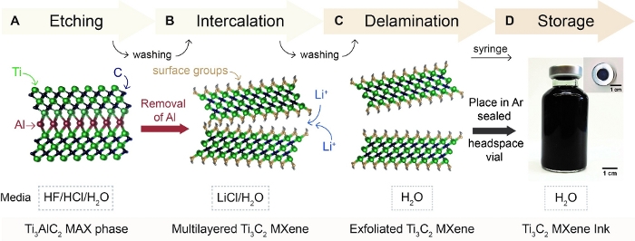
Figure 1: Schematic depicting MXene synthesis procedure. (A) Ti3AlC2 MAX is added to a selective etchant solution (HF, HCl, and DI H2O), resulting in the removal of aluminum (Al). (B) After washing the etching solution to neutral pH using DI H2O, multilayered Ti3C2 is obtained. Multilayered Ti3C2 is intercalated with Li+ from an aqueous solution of lithium chloride (LiCl). (C) After washing the intercalation reaction, sediment swelling is observed representing the exchange of Li+ with H2O. Agitation of the swollen sediment results in exfoliated (or delaminated) single- to few-layer flakes of Ti3C2 MXene in H2O. Size selection and separation of delaminated Ti3C2 MXene from multilayered Ti3C2 and Ti3AlC2 MAX phase occurs at this stage. (D) Ti3C2 MXene ink is transferred via syringe to an Argon sealed headspace vial for long-term storage. Please click here to view a larger version of this figure.
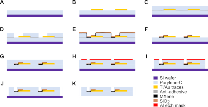
Figure 2: Schematics of the fabrication procedure for MXene microelectrode arrays. (A) Bottom parylene-C layer is deposited on a clean Si wafer. (B) Ti/Au (10 nm/100 nm) conductive traces are patterned through photolithography, e-beam deposition, and lift-off. (C) An anti-adhesive layer of 1% cleaning solution in DI H2O is applied, followed by deposition of a sacrificial parylene-C layer. (D) The sacrificial parylene-C layer is patterned through photolithography and O2 RIE etching. (E) Ti3C2 MXene is spin-coated onto the wafer, followed by e-beam deposition of 50 nm of SiO2. (F) The sacrificial parylene-C layer is lifted off, residues of cleaning solution are rinsed off, and the wafer is baked dry. (G) Top parylene-C layer is deposited. (H) An Al etch mask layer is patterned through photolithography, e-beam deposition, and lift-off to define VIAs and device outline. (I) Parylene-C over electrode contacts and surrounding devices is etched away through O2 RIE. (J) Al etch mask and SiO2 protective layer over MXene are etched away through wet etch processes. (K) Finished device is lifted off wafer. Please click here to view a larger version of this figure.
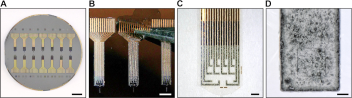
Figure 3: Photographs and optical microscopy images of MXene microelectrode arrays. (A) Photograph of a 3 inch Si wafer containing 14 completed MXene microelectrode arrays. Note the gold ring around the outer edge of the wafer, which is helpful for performing step 2.7 effectively. (B) Optical microscope image showing the peeling up of a completed device from the wafer using a small amount of DI H2O. (C) Optical microscope image showing the array of MXene microelectrodes. (D) Optical microscope image of an individual MXene electrode. Scale bars = 1 cm, 3 mm, 500 μm, 20 μm (left to right). Please click here to view a larger version of this figure.
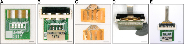
Figure 4: Interfacing the MXene microelectrode array with the adapter board. (A) PCB with pads for soldering Omnetics and ZIF connectors. (B) PCB after soldering of Omnetics and ZIF connectors. (C) Addition of polyimide layers to back side of Au bonding pads of device, to give sufficient thickness for the ZIF connector. Two layers of polyimide are added (top) and then trimmed around the edges (bottom). (D) MXene microelectrode array inserted into the ZIF connector with proper alignment. (E) Top view of MXene microelectrode array connected to adapter board and ready for a recording experiment. Scale bars = 2 mm. Please click here to view a larger version of this figure.
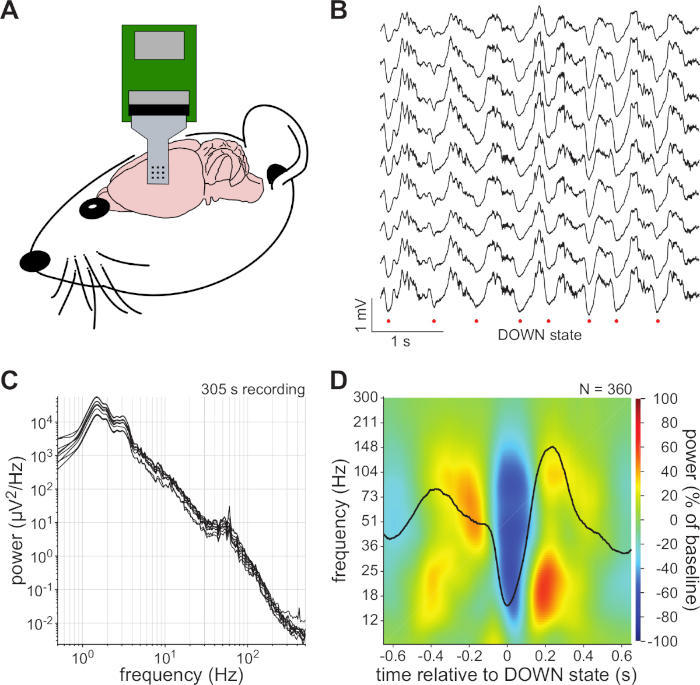
Figure 5: Representative neural recording results. (A) Illustration of placement of micro-ECoG array on cortical surface of an anesthetized rat. (B) Segment of recorded cortical activity shown for 9 electrodes. Putative cortical "down" states based on trough of the slow oscillation (1−2 Hz) are indicated by red circles. (C) Power spectral densities for each recording channel. (D) "Down" state-triggered scalogram for representative micro-ECoG channel. Note broadband power attenuation during "down" state and selective β-band (15−30 Hz) and γ-band (40−120 Hz) power amplification during "up" state. Overlaid black trace shows average slow oscillation. Please click here to view a larger version of this figure.
Discussion
The MXene synthesis and delamination procedure described in this protocol (HF/HCl/LiCl) was built from the MILD etching approach which employed a LiF/HCl (in situ HF) etchant medium26. The MILD approach allows for large Ti3C2 flakes (several µm in lateral size) to be spontaneously delaminated during washing once pH ~5−6 has been attained. Compared to etching with HF alone, this results in material with higher quality and improved material properties, such as electronic conductivity and chemical stability. The HF/HCl/LiCl method takes advantage of the MILD synthesis improvements, while additionally separating each step (etching, intercalation, and delamination) allowing for more user control.
During step 1.1, the ratio of raw materials (TiC, Al, Ti), temperature, temperature ramp rate, and time are critical to achieving the correct MAX phase. Sieving of the MAX phase prior to etching will ensure more homogenous etching. Adding the MAX phase to the etchant media (step 1.2) must be conducted slowly to prevent overheating and a general rule of 5 min per 1 g of MAX is suggested. If overheating becomes a challenge, an ice bath should be employed during addition of the Ti3AlC2 MAX phase. When washing the etching reaction to neutral pH (step 1.3), each acidic supernatant after centrifugation should be transparent. If the supernatant after centrifugation is dark or dilute green, increase the centrifuge time and/or speed to sediment material. Because the addition of LiCl to H2O is exothermic, some heating will occur (step 1.4). In this procedure, the intercalation time (step 1.4) is 12 h, although it can be modified or shortened to as little as 15 minutes. The quality of delamination (step 1.5) is specific to the quantity of water used during washing and the degree of agitation. The supernatants decanted during this step may be dilute instead of transparent. If sedimentation of material becomes a challenge, increasing the centrifuge speed/rcf should be used. It is critical to perform separation and size selection by centrifugation (step 1.5) to avoid polydisperse samples. Failure to perform this step will result in an ink that has both Ti3AlC2 MAX phase contamination and large multilayer Ti3C2 particles. During step 1.6, it is important that the headspace volume of the vial is minimized.
During the fabrication of the MXene microelectrode arrays, there are several critical steps which are essential for producing functioning, high-quality electrodes. It is important to design the first photomask such that there is a metal ring patterned around the outer edge of the wafer (step 2.2) and the second photomask such that there is a corresponding, slightly larger diameter ring which will be etched through the sacrificial parylene-C (step 2.4) layer to aid in removing the sacrificial layer. Without this ring, it can be difficult to establish an edge to begin peeling up the sacrificial parylene-C layer in step 2.7. During step 2.3, it is critical to expose the wafer to O2 plasma to allow the dilute cleaning solution to properly wet and adhere to the wafer. Failure to perform this step will result in areas of the wafer not accumulating an anti-adhesive layer, which renders the removal of the sacrificial parylene-C layer in step 2.7 impossible. During the removal of the sacrificial parylene-C layer in step 2.7, it is important to be careful to avoid scratching or damaging the bottom parylene-C layer, as this can lead to the formation of bubbles between the bottom parylene-C and the Si wafer, and subsequent delamination. If the sacrificial parylene-C layer does not peel up easily, a slightly more concentrated cleaning solution (4% in DI) can be used in step 2.3.1, or the O2 plasma exposure in step 2.3.1 can be prolonged to improve hydrophilicity of the underlying parylene-C layer.
After the fabrication is completed, properly interfacing the MXene device with the connector board is essential. The addition of two layers of polyimide tape in step 3.2 is essential to ensure proper thickness for insertion into the ZIF connector, however care should be taken to avoid accidental folding or crumpling of the thin parylene-C device while the tape is added, as it is not possible to remove the tape without damaging the device. Subsequently, proper alignment of the Au bonding pads on the MXene device with pins inside the ZIF connector (Figure 4D) is essential for forming a robust connection (step 3.3). At this stage, measuring the impedance of the MXene electrodes is helpful for troubleshooting. A 50 μm x 50 μm square MXene electrode should have an impedance magnitude near 50 kΩ at a frequency of 1 kHz in 1x PBS, and a 25 μm diameter circular MXene electrode should have an impedance magnitude near 200 kΩ under the same parameters36. An impedance significantly larger than this can indicate that the electrode is not properly connected in the ZIF connector, or that the MXene electrode is not exposed, as may happen if either the top parylene-C layer was not completely etched in step 2.10 or the SiO2 protective layer was not fully etched in step 2.11.
One limitation of this method is variability in MXene film thickness that is sometimes observed after spin-casting MXene onto the wafer. This variability can become more pronounced if electrodes are scaled up to larger areas. This limitation can be readily overcome by utilizing spray-coating instead of spin-coating to apply MXene to the wafer, representing another simple, low-cost solution processing method with which MXene, and this protocol, are compatible39.
The protocol described here presents exciting new opportunities in neuroscience and in the larger field of bioelectronics. While there has long been interest in leveraging carbon-based nanomaterials for neural microelectrodes, the incorporation of Ti3C2 MXene into such electrodes has enabled significantly simpler and more high-throughput fabrication than has been possible with other carbon-based nanomaterials. Furthermore, the outstanding properties of Ti3C2 MXene endow the electrodes with remarkably low impedance for their size, thus improving sensitivity and signal quality. A growing body of literature also describes a number of methods for micropatterning MXene, which may be adapted for fabricating MXene microelectrodes in the future, including micro-contact printing40, inkjet printing41,42, and automated scalpel engraving43. There exists great potential to extend this protocol to fabricate Ti3C2 MXene electrodes of arbitrary size and geometry for a range of biosensing applications.
Divulgazioni
The authors have nothing to disclose.
Acknowledgements
This work was supported by the National Institutes of Health (grant no. R21-NS106434), the Citizens United for Research in Epilepsy Taking Flight Award, the Mirowski Family Foundation and Neil and Barbara Smit (F.V.); the National Science Foundation Graduate Research Fellowship Program (grant no. DGE-1845298 to N.D. and B.M.); the Army Research Office (Cooperative Agreement Number W911NF-18-2-0026 to K.M.); and by the U.S. Army via the Surface Science Initiative Program at the Edgewood Chemical Biological Center (PE 0601102A Project VR9 to Y.G. and K.M.). This work was carried out in part at the Singh Center for Nanotechnology, which is supported by the National Science Foundation National Nanotechnology Coordinated Infrastructure Program (NNCI-1542153).
Materials
| 00-90 screw | McMaster-Carr | 90910A630 | Skull screw around which ground wire is wrapped |
| 128ch stimulation/recording controller | Intan Technologies | A component of the neural recording system. | |
| 175 mL polypropylene (PP) conical centrifuge tubes | Falcon | REF: 352076 | Used for washing |
| 18 position 0.5 mm pitch ZIF connector | Molex | 505110-1892 | Used to interface the flexible Parylene microelectrode array with the PCB adapter board. |
| 18 position dual row male nano-miniature (.025"/.64mm) connector | Omnetics Connector Corporation | A79008-001 | Used to interface the PCB adapter board to the recording headstage. |
| 3ML Disposable Plastic Set Transfer Graduated Pipettes | Rienar | Rienar-3ML-20PCS | Used for transferring etchant or MXene solutions |
| 50 mL polyproylene (PP) concial centrifuge tube | Falcon | REF: 352070 | Used for washing and size selection |
| Al etchant Type A | Transene | 060-0026000-QT | For removing Al etch mask layer after final Parylene-C etch. |
| Aluminum Powder, -325 Mesh, 99.5% (metals basis), particle size < 44 µm | Alfa Aesar | CAS: 7429-90-5 | Used for MAX synthesis |
| AutoCAD software | Autodesk Inc. | Design software for drawing photomasks. Free alternatives include DraftSight and LayoutEditor. | |
| Buffered Oxide Etchant 6:1 | JT Baker | 1178-03 | For removing SiO2 layer to expose MXene electrode contacts at the end of the fabrication procedure. |
| Buprenorphine SR | Wildlife Pharmaceuticals | Analgesia for rat surgery | |
| Centrifuge | Hermle | Benchmark Z 446 | Used for washing and size selection |
| Dexdomitor | Midwest Veterinary Supply | 193.13250.3 | Anesthesia for rat surgery |
| Drill burr | Fine Science Tools | 19007-07 | Burrs for drill |
| Electric drill | Foredom | K.1070 | Micromotor drill for craniotomies |
| Electron beam evaporator | Kurt J. Lesker Company | Used to evaporate Ti, Au, and SiO2 during fabrication. Most university clean rooms have this or a similar tool. | |
| Ground wire | A-M Systems | 781500 | Bare silver wire |
| Headspace Vial, glass | Supelco | REF: 27298 | Used for storing MXene solutions |
| Hydrochloric acid (12.1N) | Fisher Scientific | CAS: 7647-01-0 | Corrosive; etchant material |
| Hydrofluoric Acid, (48-51% solution in H2O) | Acros | CAS: 7664-39-3 | Etchant material |
| Jupiter II RIE system | March Plasma Systems Inc. | Planar RIE etching system used to etch the Parylene-C using O2 plasma. Most university clean rooms have a comparable planar RIE etching system. | |
| Kapton standard polyimide tape, 1/4" | DuPont | Used to add thickness to the Au bonding pad region of the flexible Parylene microelectrode array for insertion into the ZIF connector. | |
| Ketamine | Hospital of the Univ. of Penn. | Anesthesia for rat surgery | |
| KLA P-7 Stylus Profilometer | KLA Corporation | Used the measure 2D profiles to confirm complete etching through the sacrificial parylene-C layer in step 2.4.2. Most university clean rooms have this or a comparable stylus profilometer tool. | |
| Lithium chloride, 99% for analysis, anhydrous | Acros | CAS: 7447-41-8 | Hygroscopic; delamination material |
| MA6 mask aligner | Karl Suss Microtec AG | Used to align each photomask to the pattern on the wafer and expose the wafer to UV light. Most university clean rooms have this or a similar tool. | |
| Micro-90 cleaning solution | International Products Corporation | M-9050-12 | Used as the anti-adhesive layer to enable removal of the sacrificial Parylene-C layer to pattern the MXene |
| NR71-3000p photoresist | Futurrex Inc. | NR71-3000p | Negative photoresist used to define Ti/Au traces and MXene patterns in the devices. |
| Ophthalmic ointment | Midwest Veterinary Supply | 193.63200.3 | To prevent corneal drying during surgery |
| Parylene deposition system | Specialty Coating Systems | Used to evaporate thin conformal films of Parylene-C | |
| Parylene-C dimer | Specialty Coating Systems | 980130-c-01lbe | Flexible polymer used as bottom and top passivating layers for the flexible MXene devices |
| Photomasks (chrome on soda lime glass) | University of Pennsylvania | Our photomasks were produced in the University clean room using a Heidelberg DWL66+ laser writer system, however several vendors manufacture photomasks from provided design files. | |
| Povidone-iodine solution | Medline | MDS093901 | To help prevent infection around scalp incision |
| Printed Circuit Board (PCB) | Advanced Circuits | Used to interface between the MXene electrode array and the measurement electronics such as the potentiostat and the Intan recording system. Advanced Circuits and other vendors manufacture and assemble PCBs based on the provided design files. | |
| RD6 Developer | Futurrex Inc. | RD6 Developer | Used to develop NR71-3000p negative photoresist following UV exposure |
| Reference 600 potentiostat | Gamry Instruments | Used to measure the electrodes' impedance to assess quality of the devices | |
| Remover PG | MicroChem Corp. | G050200 | Used to remove NR71-3000p following metal deposition to perform lift-off patterning |
| RHS2000 Stim SPI interface cable | Intan Technologies | A component of the neural recording system. | |
| RHS2116 amplifier board | Intan Technologies | A component of the neural recording system. | |
| Si wafers | Wafer World | 2885 | Substrate for fabrication |
| Spin Coater | Cost Effective Equipment | For coating wafers with resists and applying the Micro-90 and MXene layers. Most university clean rooms have spin coaters. | |
| Stereotaxic frame | Kopf Instruments | Model 902 | For positioning the rat for neurosurgery |
| Teflon-coated magnetic stir bar | Corning | REF: 1233W95 | Used to stir during etching and intercalation |
| Titanium carbide, 99.5% (metals basis), particle size ~2 µm | Alfa Aesar | CAS: 12070-08-5 | Used for MAX synthesis |
| Titanium powder, -325 mesh, 99% (metals basis), particle size < 44µm | Alfa Aesar | CAS: 7440-32-6 | Used for MAX synthesis |
| Ultrasonic bath sonicator | Reynolds Tech | For removing metal and photoresist particles during lift-off processes to pattern metals. | |
| UV vis spectrophotometer | ThermoScientific | Evolution 201 | Used to determine concentration and observe absorption peak |
| Zetasizer, Particle Size Analysis | Malvern Panalytical | Nano ZS | Used to determine particle lateral size distibution |
Riferimenti
- Ludwig, K. A., et al. Poly(3,4-ethylenedioxythiophene) (PEDOT) polymer coatings facilitate smaller neural recording electrodes. Journal of Neural Engineering. 8 (1), 014001 (2011).
- Polikov, V. S., Tresco, P. A., Reichert, W. M. Response of brain tissue to chronically implanted neural electrodes. Journal of Neuroscience Methods. 148 (1), 1-18 (2005).
- Lecomte, A., Descamps, E., Bergaud, C. A review on mechanical considerations for chronically-implanted neural probes. Journal of Neural Engineering. 15 (3), 031001 (2017).
- Castagnola, E., et al. Smaller, softer, lower-impedance electrodes for human neuroprosthesis: a pragmatic approach. Frontiers in Neuroengineering. 7, 8 (2014).
- Nguyen, J. K., et al. Mechanically-compliant intracortical implants reduce the neuroinflammatory response. Journal of Neural Engineering. 11 (5), 056014 (2014).
- Boehler, C., Stieglitz, T., Asplund, M. Nanostructured platinum grass enables superior impedance reduction for neural microelectrodes. Biomaterials. 67, 346-353 (2015).
- Petrossians, A., Whalen, J. J., Weiland, J. D., Mansfeld, F. Surface modification of neural stimulating/recording electrodes with high surface area platinum-iridium alloy coatings. 2011 Annual International Conference of the IEEE Engineering in Medicine and Biology Society. , 3001-3004 (2011).
- Meyer, R. D., Cogan, S. F., Nguyen, T. H., Rauh, R. D. Electrodeposited iridium oxide for neural stimulation and recording electrodes. IEEE Transactions on Neural Systems and Rehabilitation Engineering. 9 (1), 2-11 (2001).
- Ferguson, J. E., Boldt, C., Redish, A. D. Creating low-impedance tetrodes by electroplating with additives. Sensors and Actuators A: Physical. 156 (2), 388-393 (2009).
- Kotov, N. A., et al. Nanomaterials for Neural Interfaces. Advanced Materials. 21 (40), 3970-4004 (2009).
- Keefer, E. W., Botterman, B. R., Romero, M. I., Rossi, A. F., Gross, G. W. Carbon nanotube coating improves neuronal recordings. Nature Nanotechnology. 3 (7), 434-439 (2008).
- Lu, Y., et al. Electrodeposited polypyrrole/carbon nanotubes composite films electrodes for neural interfaces. Biomaterials. 31 (19), 5169-5181 (2010).
- Green, R. A., Williams, C. M., Lovell, N. H., Poole-Warren, L. A. Novel neural interface for implant electrodes: improving electroactivity of polypyrrole through MWNT incorporation. Journal of Materials Science: Materials in Medicine. 19 (4), 1625-1629 (2008).
- Apollo, N. V., et al. Flexible Freestanding Neural Stimulation and Recording Electrodes Fabricated from Reduced Graphene Oxide. Advanced Functional Materials. 25 (23), 3551-3559 (2015).
- Lu, Y., Lyu, H., Richardson, A. G., Lucas, T. H., Kuzum, D. Flexible Neural Electrode Array Based-on Porous Graphene for Cortical Microstimulation and Sensing. Scientific Reports. 6 (1), 33526 (2016).
- Matarredona, O., et al. Dispersion of Single-Walled Carbon Nanotubes in Aqueous Solutions of the Anionic Surfactant NaDDBS. The Journal of Physical Chemistry B. 107 (48), 13357-13367 (2003).
- Ramesh, S., et al. Dissolution of Pristine Single Walled Carbon Nanotubes in Superacids by Direct Protonation. The Journal of Physical Chemistry B. 108 (26), 8794-8798 (2004).
- Kim, S. W., et al. Surface modifications for the effective dispersion of carbon nanotubes in solvents and polymers. Carbon. 50 (1), 3-33 (2012).
- Wang, M., et al. Nanotechnology and Nanomaterials for Improving Neural Interfaces. Advanced Functional Materials. 28 (12), 1700905 (2017).
- Wang, K., Fishman, H. A., Dai, H., Harris, J. S. Neural Stimulation with a Carbon Nanotube Microelectrode Array. Nano Letters. 6 (9), 2043-2048 (2006).
- Ansaldo, A., Castagnola, E., Maggiolini, E., Fadiga, L., Ricci, D. Superior Electrochemical Performance of Carbon Nanotubes Directly Grown on Sharp Microelectrodes. ACS Nano. 5 (3), 2206-2214 (2011).
- Nimbalkar, S., et al. Ultra-Capacitive Carbon Neural Probe Allows Simultaneous Long-Term Electrical Stimulations and High-Resolution Neurotransmitter Detection. Scientific Reports. 8, 6958 (2018).
- Anasori, B., Lukatskaya, M., Gogotsi, Y. 2D metal carbides and nitrides (MXenes) for energy storage. Nature Reviews Materials. 2, 16098 (2017).
- Anasori, B., Gogotsi, Y. . 2D Metal Carbides and Nitrides (MXenes): Structure, Properties and Applications. , (2019).
- Naguib, M., et al. Two-Dimensional Nanocrystals Produced by Exfoliation of Ti3AlC2. Advanced Materials. 23 (37), 4248-4253 (2011).
- Alhabeb, M., et al. Guidelines for Synthesis and Processing of Two-Dimensional Titanium Carbide (Ti3C2Tx MXene). Chemistry of Materials. 29 (18), 7633-7644 (2017).
- Ghidiu, M., Lukatskaya, M. R., Zhao, M. Q., Gogotsi, Y., Barsoum, M. W. Conductive two-dimensional titanium carbide ‘clay’ with high volumetric capacitance. Nature. 516 (7529), 78-81 (2014).
- Lukatskaya, M. R., et al. Ultra-high-rate pseudocapacitive energy storage in two-dimensional transition metal carbides. Nature Energy. 2, 17105 (2017).
- Zhu, Y., et al. Carbon-Based Supercapacitors Produced by Activation of Graphene. Science. 332 (6037), 1537-1541 (2011).
- Heon, M., et al. Continuous carbide-derived carbon films with high volumetric capacitance. Energy & Environmental Science. 4 (1), 135-138 (2011).
- Yang, X., Cheng, C., Wang, Y., Qiu, L., Li, D. Liquid-mediated dense integration of graphene materials for compact capacitive energy storage. Science. 341 (6145), 534-537 (2013).
- Zhang, C. J., et al. Transparent, Flexible, and Conductive 2D Titanium Carbide (MXene) Films with High Volumetric Capacitance. Advanced Materials. 29 (36), 1702678 (2017).
- Han, X., et al. 2D Ultrathin MXene-Based Drug-Delivery Nanoplatform for Synergistic Photothermal Ablation and Chemotherapy of Cancer. Advanced Healthcare Materials. 7 (9), 1701394 (2018).
- Dai, C., et al. Biocompatible 2D Titanium Carbide (MXenes) Composite Nanosheets for pH-Responsive MRI-Guided Tumor Hyperthermia. Chemistry of Materials. 29 (20), 8637-8652 (2017).
- Xu, B., et al. Ultrathin MXene-Micropattern-Based Field-Effect Transistor for Probing Neural Activity. Advanced Materials. 28 (17), 3333-3339 (2016).
- Driscoll, N., et al. Two-Dimensional Ti3C2 MXene for High-Resolution Neural Interfaces. ACS Nano. 12 (10), 10419-10429 (2018).
- Sessolo, M., et al. Easy-to-Fabricate Conducting Polymer Microelectrode Arrays. Advanced Materials. 25 (15), 2135-2139 (2013).
- Shuck, C. E., et al. Effect of Ti3AlC2 MAX Phase on Structure and Properties of Resultant Ti3C2Tx MXene. ACS Applied Nano Materials. 2 (6), 3368-3376 (2019).
- Hantanasirisakul, K., et al. Fabrication of Ti3C2Tx MXene Transparent Thin Films with Tunable Optoelectronic Properties. Advanced Electronic Materials. 2 (6), 1600050 (2016).
- Xu, B., et al. Ultrathin MXene-Micropattern-Based Field-Effect Transistor for Probing Neural Activity. Advanced Materials. 28 (17), 3333-3339 (2016).
- Zhang, C., et al. Additive-free MXene inks and direct printing of micro-supercapacitors. Nature Communications. 10 (1), 1795 (2019).
- Quain, E., et al. Direct Writing of Additive-Free MXene-in-Water Ink for Electronics and Energy Storage. Advanced Materials Technologies. 4 (1), 1800256 (2019).
- Salles, P., Quain, E., Kurra, N., Sarycheva, A., Gogotsi, Y. Automated Scalpel Patterning of Solution Processed Thin Films for Fabrication of Transparent MXene Microsupercapacitors. Small. 14 (44), 1802864 (2018).
