JoVE Science Education
Electrical Engineering
This content is Free Access.
JoVE Science Education Electrical Engineering
DC/DC Boost Converter
  • 00:06Visão Geral
  • 00:58Principles of Boost Converters
  • 05:01Board Setup
  • 07:12Boost Converter Testing with Variable Input
  • 08:38Boost Converter Testing with Variable Duty Ratio
  • 09:53Resultados
  • 11:02Applications
  • 11:56Summary

DC/DC-Aufwärtswandler

English

COMPARTILHAR

Visão Geral

Quelle: Ali Bazzi, Department of Electrical Engineering, University of Connecticut, Storrs, CT.

Boost-Konverter bieten eine vielseitige Lösung für Intensivierung Gleichspannungen in vielen Anwendungen, wo eine Gleichspannung muss erhöht werden, ohne die Notwendigkeit, es zu AC konvertieren, mit einem Transformator und dann die Trafoleistung beheben. Boost-Konverter sind step-up-Wandler, die eine Induktivität als Energiespeicher zu verwenden, die die Ausgabe mit zusätzlicher Energie neben der DC-Eingangsquelle unterstützt. Dies bewirkt, dass die Ausgangsspannung zu erhöhen.

Das Ziel dieses Experiments ist, unterschiedliche Eigenschaften eines Boost-Konverter zu studieren. Die Step-up-Fähigkeit des Konverters wird unter kontinuierlichen Wärmeleitung Modus (CCM) beobachtet werden, wo die aktuellen Induktivität ungleich Null ist. Open-Loop Betrieb mit einer manuell-Set Tastverhältnis wird verwendet. Eine Annäherung an die Input-Output-Beziehung wird beobachtet.

Princípios

Ein Boost-Konverter stützt sich auf gespeicherte Energie in die Induktivität L, zur Energieversorgung von der Output-Seite, wo die Last getragen wird, zusätzlich eine DC-Quelle ist die wichtigste Energiequelle. Das grundlegende Konzept hinter Boost-Konverter-Betrieb ist, dass eine Induktivität seine Spannung Polarität um Stromfluss aufrechtzuerhalten umkehren wird. Wie dargestellt in Abb. 1a für eine einfache Boost-Konverter-Schaltung, wenn der Schalter aktiviert ist, für einen Arbeitszyklus D von den Schaltzeitraum T, Induktor Spannung, die VL aufbaut. Wenn der Schalter ausgeschaltet ist, aktuelle Induktivität hat weiterhin fließt und daher wird der Induktor Spannung Polarität spiegeln, um die Eingangsspannung Vdehinzufügen.

Jedoch, wenn der Schalter eingeschaltet ist, die Last ist kurzgeschlossen und die Ausgangsspannung ist Null, was nicht erwünscht ist. Daher ist eine Sperrdiode in der Output-Seite hinzugefügt, wie in Abb. 1 gezeigt, um verhindern, dass die Last kurzgeschlossen wird. Diese Diode löst noch nicht das Problem der Last keine Spannung zu sehen, wenn der Schalter aktiviert, ist also ein Kondensator hinzugefügt wird, wie in Abb. 1 dargestellt, um die Belastung in der Phase mit notwendigen Strom liefern wenn der Schalter eingeschaltet ist. Beachten Sie, dass bei der Schalter ist, die Diode leuchtet (Reverse voreingenommen), und umgekehrt. Die durchschnittliche Ausgangsspannung bezieht sich somit auf die Eingangsspannung als: < V,> = Vde/(1-D).

Figure 1
Abbildung 1. Schritte zum Aufbau einer Hochsetzsteller

Im weiteren Verlauf dieses Experiment wird es gezeigt, dass die durchschnittliche Ausgangsspannung steigt das Tastverhältnis, D. Dies gilt, da die Ausgangsspannung Spannung Beziehung Eingabe umgekehrt proportional zur –D ist, und somit die Ausgangsspannung und D eine positive Korrelation haben.

Beachten Sie, dass die Gleichung dargestellt für eine ideale Hochsetzsteller ist und scheinen kann, als ob ein D = 1 ergibt unendlich Ausgangsspannung, aber das ist nicht wahr. In Wirklichkeit beginnen parasitären Elementen und Widerstände in der Boost-Konverter Ursache D nach welche parasitäre Effekte auf rund 70-80 % begrenzt werden, dominieren Schaltung Betrieb und verursachen erhebliche Spannung abfällt. An diesem Punkt beginnt die Ausgangsspannung zu verringern, da D erhöht. Mit höher Schaltfrequenzen, verringert sich die Welligkeit der Spannung am Ausgang seit der Spannung aufladen und Entladen Zeiten an den Kondensator werden mit einer verringerten Schaltfrequenz deutlich kürzer.

Procedimento

Achtung: Dieses Experiment soll die Ausgangsspannung kleiner als 50V DC zu begrenzen. Verwenden Sie nur Pflicht-Verhältnisse, Frequenzen, Eingangsspannung oder Lasten, die hier gegeben werden. Dieses Experiment wird die DC-DC Konverter Verpflegung HiRel Systeme nutzen. http://www.hirelsystems.com/Shop/Power-Pole-Board.HTML Informationen über den Vorstand Betrieb finden Sie in diesem Video Sammlungen “Introduction to HiRel Board.” Das hier gezeigte Verfahren gilt für jede einfache Boost Konverter Schaltung, die auf Proto-Boards, Frühstück Bretter oder Leiterplatten aufgebaut werden kann. (1) Board-Setup: ±12 Signal anschließen an der Buchse “DIN” aber halten “S90” aus. Stellen Sie sicher, dass die PWM-Steuerung-Selektor auf die offene Regelkreis-steht. Die DC-Stromversorgung auf 10 V eingestellt. Halten Sie die Ausgabe aus dem Vorstand vorerst getrennt. Vor dem Anschließen des Last Widerstands, passen Sie an, um 20 Ω. Bauen Sie die Schaltung in Bild 2 gezeigt, indem die untere MOSFET, obere Diode und BB Magnettafel. Notieren Sie sich die Induktivität Wert auf dem Board gezeigt. Schließen Sie “RL”über “V1 +” und “Com” Beachten Sie, dass die Input- und Output-Anschlüsse im Vergleich zu denen in der Buck-Konverter-Experiment gekippt werden. NIE trennen die Last während des Experiments als Boost-Konverter kann instabil werden und verursachen Schäden an den Vorstand. Sicherstellen der Schalter Array für MOSFET Auswahl (untere MOSFET), PWM-Auswahl und anderen Einstellungen richtig Funktionskreis wie in Abb. 2 zu erreichen sind. Abbildung 2 . Wandlerschaltung steigern 2. Einstellen der Einschaltdauer und Schalthäufigkeit Verbinden Sie die Differenzialfühler über die Gate-Source der unteren MOSFETs. Schalten Sie “S90.” Der Anwendungsbereich sollte ein Schaltsignal angezeigt. Passen Sie die Signal-Zeit-Achse um zwei oder drei Punkte zu sehen. Stellen Sie die Frequenz Potentiometer um eine Frequenz von 100 kHz (Periode von 10 µs) zu erreichen. Passen Sie das Dienst Verhältnis Potentiometer um eine 10 % Tastverhältnis (pünktlich von 1 µs) zu erreichen. (3) die Prüfung für die Variable Eingabe Hochsetzsteller Schließen Sie die Eingabe DC-Stromversorgung, die bereits bei 10 V, “V2 +” und “Com” eingestellt Schließen Sie die differenzielle Sonde zur Messung des Induktors zurzeit “CS5.” Verbinden Sie die andere Sonde über die Last. Stellen Sie sicher, dass der Boden-Anschluss für “Com” Erfassen Sie die Wellenformen zu und Messen Sie die Ausgang Spannung bedeuten, Induktor Stromwelligkeit und Induktivität aktuelle bedeuten. Erfassen der Eingangsstrom und Spannung Lesungen auf dem DC-Netzteil. Passen Sie die Eingangsspannung 8 V, 12 V und 14 V, und wiederholen Sie die oben genannten Schritte für jede dieser Spannungen. Trennen Sie den Eingang DC liefern und passen Sie die Leistung auf 10 V. (4) die Prüfung für Variable Einschaltverhältnis Hochsetzsteller Verbinden Sie die Differenzialfühler über das Tor zur Quelle des unteren MOSFET. Verbinden Sie die andere Sonde über die Last. Stellen Sie sicher, dass der Boden-Anschluss für “Com” Schließen Sie die DC-Eingangsspannung “V2 +” und “Com” Erfassen Sie die Wellenformen zu und Messen Sie die Ausgang Spannung bedeuten und Einschaltzeit der Gate-Source-Spannung (auch das Tastverhältnis). Erfassen der Eingangsstrom und Spannung Lesungen auf dem DC-Netzteil. Passen Sie das Einschaltverhältnis um 20 %, 40 % und 60 %. Wiederholen Sie die oben genannten Schritte für jede dieser drei Pflicht-Verhältnisse. Setzen Sie das Einschaltverhältnis auf 10 %. Trennen Sie den DC-Eingangsspannung. (5) Konverter Tests für Variable Schaltfrequenz zu steigern Verbinden Sie die Differenzialfühler über das Tor zur Quelle des unteren MOSFET. Verbinden Sie die andere Sonde über die Last mit dem Boden-Stecker angeschlossen für “Com” Schließen Sie die DC-Eingangsspannung “V2 +” und “Com” Passen Sie die Schaltfrequenz bis 70 kHz. Erfassen Sie die Wellenformen zu und Messen Sie die Ausgang Spannung bedeuten und Einschaltzeit der Gate-Source-Spannung (auch das Tastverhältnis). Aufzeichnung der Eingangsstrom und lesen auf die DC Spannung liefern. Passen Sie die Schaltfrequenz bis 40 kHz, 20 kHz und 10 kHz (oder mindestens möglich 10 kHz erreichbar). Wiederholen Sie die obigen Schritte für alle diese drei Schaltfrequenzen. Schalten Sie den DC-Eingangsspannung und “S90”, und dann zerlegen Sie die Schaltung zu.

Resultados

The boost converter output-input voltage relationship is proportional to the duty cycle in the sense that higher D will yield higher output voltages for a given input voltage. If the input voltage is Vdeand the output voltage is Vout, Vout/Vde= 1/(1-D), where 0≤D≤ 100%. Therefore, for an input voltage of 10 V, Vout≈ 12.5 V for D = 20%, Vout 16.67 V for D= 40%, and Vout≈ 25 V for D = 60%.

Nevertheless, the output voltage will be lower than expected from the ideal relationship, which is linear with the duty ratio. The main reason is that the ideal converter model from which the Vout/Vde relationship can be derived does not account for non-idealities and voltage drops in the converter. Theoretically, as D→100%, Vout→∞; practically, a theoretical limit on the boosting capability is around 3-4x the input voltage, and after a certain level of D, the output voltage of the converter starts to drop rather than being boosted due to parasitic and non-ideal elements in a real converter.

Applications and Summary

Boost converters are very common in solar photovoltaic applications where the input voltage from the solar panel varies with weather conditions and available solar energy, and a boost converter can always boost from the PV panel voltage. Power factor correction to improve power quality as seen from the utility grid with power electronic loads which may require significant reactive power, e.g. motors, is another major application of boost converters.

Transcrição

Boost converters are used in electronics to generate a DC output voltage that is greater than the DC input, therefore boosting up the supply voltage. Boost converters are often used in power supplies for white LEDs, battery packs for electric automobiles, and many other applications. A boost converter stores energy in an inductor’s magnetic field and transfers it to a load with a switching circuit. The transfer of energy from the inductor’s magnetic field enables the increase in DC output in a single stage. This video will illustrate the construction of a boost converter and investigate how changing the converter’s operating condition affects its output voltage.

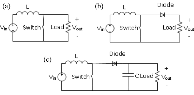
This simple boost converter circuit consists of an input DC voltage source connected to an inductor and a switch. The switch may be a bipolar transistor, a MOSFET or, other similar electronic device that alternately connects and disconnects the inductor from the common line of the power supply. A blocking diode connects the inductor to a capacitor which filters the ripple in the output voltage. Increasing the capacitance decreases the ripple. For a sufficiently large capacitance the output becomes a steady DC voltage. A digital pulse train opens or closes the switch. The pulse has a duty ratio which is the ratio of the on time to the period. The duty ratio may vary from zero or increase up to one with more and more on time. When the pulse is on, the switch closes and the inductor is connected across the supply voltage. In this state, the inductor terminal connected to the output of the power supply has the higher potential and the terminal connected to the common has the lower potential. Now current flows through the inductor increasing linearly with time for sufficiently high switching frequencies. During this time the inductor voltage is defined to be positive because the slope of the current versus time is positive. The inductor stores energy proportional to the square of the current in its magnetic field. The longer the inductor is connected to the power supply, the more current increases and the more energy it stores. When the switch opens, current through the inductor must continue flowing in the same direction. This current also decreases because the inductor now gives up energy to the load. The inductor voltage becomes negative because the slope of current versus time is negative. As a result, the inductor’s polarity flips and now adds to input voltage “V in” producing a higher potential at the output. The circuit in this state, forward biases the diode and the inductor discharges current, some going to the load, and some going to the capacitor which then stores the charge. When the switch closes again the diode becomes reverse biased disconnecting the inductor from the output and preventing a short circuit of the load. During this time the inductor recharges and in its place the capacitor provides current to the load. This cycle of capacitor charging and discharging produces an average output voltage with some amount of ripple. At sufficiently high switching frequencies, the capacitor’s charge and discharge times are short and the output reaches a steady state voltage with relatively little ripple. This switching cycle repeats indefinitely and is the basis of boost converter operation. Ideally the average output voltage increases as the duty ratio increases and a duty ratio of one generates infinite voltage. However parasitic elements and resistances in the boost converter limit useful values of D to a maximum of about 0.7 or 0.8. If D is sufficiently large, parasitic effects dominate circuit operation and output voltage decreases even as D continues to increase. In the following experiments we will study how a boost converter steps up voltage in continuous conduction mode, also called CCM, a condition when the inductor operates at all times with non zero current.

The output voltage in this experiment is limited to 50 volts DC or less. Use only the specified duty cycles, frequencies, input voltages, and loads. These experiments utilize the HiRel Systems Power Pole Board which is designed for experimentation with different DC to DC converter circuit topologies. With signal supply switch S90 turned off, plug the +/- 12 volt signal supply into den connector J90. Set the PWM control selection jumpers J62 and J63 to the open loop position. Adjust the DC power supply to positive 10 volts but do not connect the power supply output to the board. Next build the circuit as shown with the lower MOSFET, the upper diode, and the BB magnetic board. Record the value of the inductor on the BB magnetic board. The load resistor is a power potentiometer. Use a multi meter to measure it’s resistance while adjusting it to 20 ohms. Then connect the potentiometer between terminals V1+ and COM. Set switch selector bank S30 as follows: PWM to bottom MOSFET, use onboard PWM, and switched load off. Connect the oscilloscope’s differential probe between terminal 16 which is the gate of the lower MOSFET and terminal 12 which is the source. Turn on switch S90. The pulse train that drives the MOSFET should appear on the scope’s screen. Select the scope’s time axis to display several periods of this wave form. Set frequency adjustment potentiometer RV60 to produce a switching frequency of 100 kilohertz. Set duty ratio potentiometer RV64 so the pulses have an on time of one microsecond which corresponds to a duty ratio of 0.1.

Connect the DC power supply to input terminals V2+ and COM. To measure the inductor current connect the differential scope probe between terminals CS5 and COM. To measure the voltage across load resistor RL, connect the other differential probe between terminals V1+ and COM. The output voltage should be a triangle wave. The upward ramps occur when the boost convertor switch is open and the inductor is transferring energy to the load. The downward ramps occur when the switch is closed, the inductor is disconnected from the output, and the capacitor is supplying energy to the load. The inductor current is a triangle wave which ramps up linearly during the on time of the pulse train, then ramps down linearly during the off time. The offset is the average current. Using the scope’s built in measurement functions, measure the mean value of the output voltage and the mean value of the inductor current. Repeat these steps with the input DC power supply set to eight, 12, and 14 volts. For a fixed duty ratio as the input voltage increases the output voltage of an ideal boost converter should increase proportionally.

This part of the experiment measures the duty ratio of the pulse train instead of the inductor current. Connect the scope probes between terminals 16 and 12 which are the gate and source of the lower MOSFET respectively. Connect the input DC power supply to terminals V2+ and COM. Like before, the output voltage is a triangle wave resulting from the inductor and capacitor alternately supplying current to the load. The gate source voltage of the MOSFET is a digital pulse train with a frequency of 100 kilohertz, a period of 10 microseconds, and an on time of one microsecond. Measure the mean value of the output voltage and the on time of the gate to source voltage along with the input current and voltage readings from the DC power supply. Repeat this test after adjusting duty ratio potentiometer RV64 so the pulse stream has an on time of two, four, and six microseconds, which correspond to duty ratios of 0.2, 0.4, and 0.6 respectively.

As duty ratio D increases, the output voltage of the boost converter also increases. Ideally if D has a value of 0.2 then an input of 10 volts generates an output of about 12.5 volts. If D is 0.4 then the output would be about 16.6 volts. If D is 0.6 then the output would be about 25 volts. In general, the output voltage is less than expected from the ideal relationship because parasitic elements create non ideal voltage drops and unaccounted energy loss. As the duty ratio approaches one, the theoretical output voltage becomes infinitely large. In reality, the output voltage is limited to about three or four times the input voltage and the influence of parasitic and non ideal components causes the output voltage to decrease after D becomes sufficiently high.

Boost converters generate an output voltage that is greater than the input voltage and many applications incorporate them to increase flexibility in the choice of power sources. The voltage from a solar panel changes with the position of the sun, weather conditions, and shade. Boost converters are commonly used to step up the variable output of a solar panel array to provide a consistent voltage to feed into an electrical grid. Battery powered systems are frequently used to power devices without the use of a power cord. In order to achieve the necessary higher output voltage, battery cells are often stacked. This can take up a lot of space if many cells are needed to reach the desired output. Instead, boost converters are used to step up the voltage while conserving space.

You have just watched Jove’s Introduction to Boost Converters. You should now understand how boost converters work and how adjusting input voltage, duty ratio, and frequency affects the output voltage. Thanks for watching.

Tags

Cite This
JoVE Science Education Database. JoVE Science Education. DC/DC Boost Converter. JoVE, Cambridge, MA, (2023).