Summary

電子衝撃イオン化のためのシャープフィールドエミッションポイントの電気化学エッチングとキャラクタリゼーション

Published: July 12, 2016
doi:

Summary

A method for electrochemically etching field emission tips is presented. Etching parameters are characterized and the operation of the tips in field emission mode is investigated.

Abstract

A new variation of the drop-off method for fabricating field emission points by electrochemically etching tungsten rods in a NaOH solution is described. The results of studies in which the etching current and the molarity of the NaOH solution used in the etching process were varied are presented. The investigation of the geometry of the tips, by imaging them with a scanning electron microscope, and by operating them in field emission mode is also described. The field emission tips produced are intended to be used as an electron beam source for ion production via electron impact ionization of background gas or vapor in Penning trap mass spectrometry applications.

Introduction

鋭い先端又は点が長くかかる電界イオン顕微鏡(FIM)1と、走査トンネル顕微鏡(STM)2、及び様々な材料の鋭い先端を製造するための技術の範囲と顕微鏡の用途に使用されている3が開発されてきました。これらの鋭い先端はまた、それらに高電圧を印加することによって電界放出点(のFEP)として動作し、便利な電子線源として機能することができます。そのようなソースとしての1つの用途は、電子衝撃イオン化(EII)を介して製造イオンです。 FEPは、熱放射体によって生成される温度変動が望ましくない用途において特に有利です。例えば、高精度の背景ガス又は蒸気のEIIを介してイオンの生成は、4,5トラップペニング。

FEPを製造するための簡単​​な方法は、電気化学的に水酸化ナトリウム(NaOH)溶液中のタングステン棒をエッチングすることです。この技術はで実装するのが比較的簡単です控えめな機器とはかなり再現性及び信頼性があることが示されています。多くの方法が文献に記載されており、これらの技術の改良は、6を引き続き表示され。ここでは、NaOH溶液中のタングステンチップの電気化学的エッチングのための方法を説明します。我々の方法は、ラメラドロップオフ技術7,8と浮遊層技術9,10のバリエーションです。これらの2つの方法のようにそれは、単一のエッチング工程からの2つの先端を製造することができます。先端部をエッチングするための実験装置の写真を図1に示されています。

図1
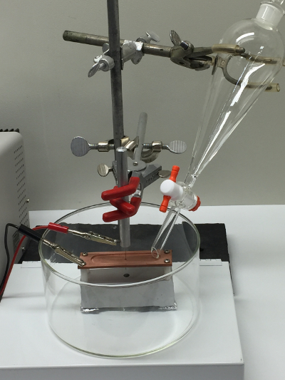
図1.エッチング装置。NaOH溶液でタングステン棒の電気化学エッチングに用いる実験装置の写真。 クリックしてくださいここで、この図の拡大版を表示します。

NaOH水溶液ベースタングステンの電気化学的エッチングは、二段階のプロセスを介して起こります。まず、中間タングステン酸化物が形成され、第二に、これらの酸化物は、非電気化学的に可溶性タングステン酸塩アニオンを形成するために溶解されます。このプロセスは、2つの反応によって、簡略化された形で、説明されています

(1)W + 60時間 →3(S)+ 3H 2 O + 6eのWO – 、および

(2)3(S)+ 2OH WO →WO 4 2- + H 2 O.

エッチング電流および使用されるNaOH溶液のモル濃度は、タングステン棒を介してエッチングするのに必要な時間と電圧に影響を与えます。これらの効果の研究を提示し、議論されています。さらに重要なことは、エッチングパラメータのような、電界放出モードでの動作について、先端の幾何学的形状に影響を与えると。のジオメトリ我々が生成先端は走査型電子顕微鏡(SEM)を用いてそれらを画像化することを特徴としました。これらの画像は、例えば、先端半径を推定することができます。さらに、チップは、それらに数キロボルトに典型的には数百ボルトの負の電圧を印加し、得られた電子放出電流を監視することにより、電界放出モードで操作しました。電界放出電流との関係は、I、バイアス電圧を印加し、Vは 、ファウラーノルドハイム方程式11によって記述することができます

(3)I = AV 2電子-Cr EFF / Vを

R effはチップの有効半径であり、Aは定数であり、Cは、第二ファウラーノルドハイム定数式9 、Bにおける= 6.83 eVで 3/2 V / nmで、030eq11.jpg "/>は、タングステンの仕事関数(あります式11 ≈4.5 eV)で、kは、幾何学(K≈5)に依存する因子であり、かつ式12ノルドハイム画像補正項は(あります式12 ≈1)12。したがって、チップの有効半径は、バイアス電圧の関数として、電子電流を測定することによって決定することができます。具体的には、LNのいわゆるファウラー-ノルドハイム(FN)プロット(I / V 2)1 / Vの傾きから求めることができます。

Protocol

1.電気化学エッチング 実験の設定 装置 注:電気化学的にエッチングするセットアップは、標準的な0が必要です – 30 Vの直流(DC)ベンチトップ電源と適切なケーブル、電気絶縁性のグリップとの分液漏斗、幅広いベースのガラスビーカー、および標準ロッドとユーティリティクランプを。小ねじ、絶縁スタンドオフ、およびワニ口クリップも必要…

Representative Results

エッチングパラメータの検討 エッチングプロセスの間に電源が定電流モードで動作されます。若干タングステン棒、この定電流増加を維持するために必要な電圧(によるロッドの抵抗の増加に)エッチングされます。先端が通ってすべての道をエッチングする際に電流がほぼゼロに低下します。小さな電流?…

Discussion

我々は、電気化学的にNaOH溶液の急激な電界放出点(のFEP)をエッチングし、電界放出モードでそれらを操作することによってのFEPをテストするために簡単な手順を記載しています。記載のエッチング手順は、既存の技術・ラメラドロップオフ手法7,8と浮遊層技術の9,10のバリエーションです。しかし、前述の方法よりも実施するのがより便利で信頼性の高いことが判明しまし?…

Disclosures

The authors have nothing to disclose.

Acknowledgements

We acknowledge the services of Stanley Flegler, Carol Flegler, and Abigail Tirrell at the MSU Center for Advanced Microscopy. We thank Ray Clark and Mark Wilson for technical assistance with the set-up of the electrochemical etching apparatus. Earlier contributions from Anne Benjamin, Georg Bollen, Rafael Ferrer, David Lincoln, Stefan Schwarz and Adrian Valverde, and technical assistance from John Yurkon are also acknowledged. This work was partially supported by the National Science Foundation contract no. PHY-1102511 and PHY-1307233, Michigan State University and the Facility for Rare Isotope Beams, and Central Michigan University.

Materials

Tungsten Rod 0.020" x 12" ESPI Metals http://www.espimetals.com/index.php/online-catalog/467-Tungsten  3N8 Purity
NaOH salt Cole-Parmer Item # WU-88404-71 100 g
Separatory funnel Cole-Parmer Item# WU-34506-03 250 mL 
DC Power supply BK Precision 1672 Triple Output 0 – 32 V, 0 – 3 A DC Power Supply
Acetone Cole-Parmer Item# WU-88000-68 500 mL
Data Acquisition Card National Instruments NI PXI-6221 16 AI, 24 DIO, 2 AO
Relay Magnecraft 276 XAXH-5D 7 A, 30 V DC Reed Relay
6-way 6" conflat flange cross Kurt J Lesker C6-0600
6" to 2-3/4" conflat zero length reducer flange  (x3) Kurt J Lesker RF600X275
2-3/4" conflat flange SHV feedthrough Kurt J Lesker IFTSG041033
2-3/4" conflat flange BNC feedthrough Kurt J Lesker IFTBG042033
2-3/4" conflat flange linear feedthrough MDC 660006, REF# BLM-275-2
6" conflat flange blankoff Kurt J Lesker F0600X000N
6" conflat flange window Kurt J Lesker VPZL-600
HV Power supply Keithley Instruments Keithley Model #2290-5 0 – 5 kV DC HV Power Supply
Picoammeter Keithley Instruments Keithley Model #6485
Faraday Cup Beam Imaging Solutions Model FC-1 Faraday Cup

References

  1. Muller, E. W., Bahadur, K. Field Ionization of Gases at a Metal Surface and the Resolution of the Field Ion Microscope. Phys. Rev. 102, 624 (1956).
  2. Binnig, G., Rohrer, H. Scanning Tunneling Microscopy. Helv. Phys. Acta. 55, 726-735 (1982).
  3. Melmed, A. J. The art and science and other aspects of making sharp tips. J. Vac. Sci. Technol. B. 9, 601-608 (1990).
  4. Shi, W., Redshaw, M., Myers, E. G. Atomic masses of 32,33S, 84,86Kr, and 129,132Xe with uncertainties 0.1 ppb. Phys. Rev. A. 72, 022510 (2005).
  5. Van Dyck, R. S., Zafonte, S. L., Van Liew, S., Pinegar, D. B., Schwinberg, D. B. Ultraprecise Atomic Mass Measurement of the α particle and 4He. Phys. Rev. Lett. 92, 220802 (2004).
  6. Hobara, R., Yoshimoto, S., Hasegawa, S., Sakamoto, K. Dynamic electrochemical-etching technique for tungsten tips suitable for multi-tip scanning tunneling microscopes. e-J. Surf. Sci. Nanotechnol. 5, 94-98 (2007).
  7. Klein, M., Schwitzgebel, G. An improved lamellae drop-off technique for sharp tip preparation in scanning tunneling microscopy. Rev. Sci. Instrum. 68, 3099-3103 (1997).
  8. Kerfriden, S., Nahlé, A. H., Campbell, S. A., Walsh, F. C., Smith, J. R. The electrochemical etching of tungsten STM tips. Electrochim. Acta. 43, 1939-1944 (1998).
  9. Lemke, H., Göddenhenrich, T., Bochem, H. P., Hartmann, U., Heiden, C. Improved microtips for scanning probe microscopy. Rev. Sci. Instrum. 61, 2538-2538 (1990).
  10. Song, J. P., Pryds, N. H., Glejbøl, K., Mørch, K. A., Thölén, A. R., Christensen, L. N. A development in the preparation of sharp scanning tunneling microscopy tips. Rev. Sci. Instrum. 64, 900-903 (1993).
  11. Fowler, R. H., Nordheim, L. Electron Emission in Intense Electric Fields. Proc. R. Soc. Lond. A. , 119-173 (1928).
  12. Kim, Y. -. G., Choi, E. -. H., Kang, S. -. O., Cho, G. Computer-controlled fabrication of ultra-sharp tungsten tips. J. Vac. Sci. Technol. B. 16, 2079 (1998).
  13. Brown, K. L., Tautfest, G. W. Faraday-Cup Monitors for High-Energy Electron Beams. Rev. Sci. Instrum. 27, 696 (1956).
  14. Redshaw, M., et al. Fabrication and characterization of field emission points for ion production in Penning trap applications. Int. J. Mass Spectrom. 379, 187-193 (2015).
  15. Ibe, J. P., et al. On the electrochemical etching of tips for scanning tunneling microscopy. J. Vac. Sci. Technol. A. 8, 3570 (1990).
  16. Ekvall, I., Wahlström, E., Claesson, D., Olin, H., Olsson, E. Preparation and characterization of electrochemically etched W tips for STM. Meas. Sci. Technol. 10, 11-18 (1999).
  17. Schiller, C., Koomans, A. A., van Rooy, T. L., Schönenberger, C., Elswijk, H. B. Decapitation of tungsten field emitter tips during sputter sharpening. Surf. Sci. 339, L925-L930 (1995).
check_url/54030?article_type=t

Play Video

Cite This Article
Van Well, T. L., Redshaw, M., Gamage, N. D., Kandegedara, R. M. E. B. Electrochemical Etching and Characterization of Sharp Field Emission Points for Electron Impact Ionization. J. Vis. Exp. (113), e54030, doi:10.3791/54030 (2016).

View Video