Summary

原子纳米结构可追溯制造

Published: July 17, 2015
doi:

Summary

We report a protocol for combining the atomic metrology of the Scanning Tunneling Microscope for surface patterning with selective Atomic Layer Deposition and Reactive Ion Etching. Using a robust process involving numerous atmospheric exposures and transport, 3D nanostructures with atomic metrology are fabricated.

Abstract

Reducing the scale of etched nanostructures below the 10 nm range eventually will require an atomic scale understanding of the entire fabrication process being used in order to maintain exquisite control over both feature size and feature density. Here, we demonstrate a method for tracking atomically resolved and controlled structures from initial template definition through final nanostructure metrology, opening up a pathway for top-down atomic control over nanofabrication. Hydrogen depassivation lithography is the first step of the nanoscale fabrication process followed by selective atomic layer deposition of up to 2.8 nm of titania to make a nanoscale etch mask. Contrast with the background is shown, indicating different mechanisms for growth on the desired patterns and on the H passivated background. The patterns are then transferred into the bulk using reactive ion etching to form 20 nm tall nanostructures with linewidths down to ~6 nm. To illustrate the limitations of this process, arrays of holes and lines are fabricated. The various nanofabrication process steps are performed at disparate locations, so process integration is discussed. Related issues are discussed including using fiducial marks for finding nanostructures on a macroscopic sample and protecting the chemically reactive patterned Si(100)-H surface against degradation due to atmospheric exposure.

Introduction

由于纳米技术变得在各种各样领域,认识结构更重要形成增益重要性,特别是在光刻和电子领域。强调计量的重要性在纳米尺度,特别在低于10纳米尺度,但是应当指出,在仅1纳米的特征尺寸的变化表示的分数变化至少10%。该变型可以具有对器件的性能和材料性质显著影响1,2 – 。4使用合成方法,非常精确地形成单独的特征,例如量子点或其它复杂分子可被制造,2,5,6-但通常缺乏相同精度在功能布局和方向,尽管为了提高大小和位置的控制工作。本文阐述的用于制造纳米结构邻近的原子尺寸精度和特征放置原子精度,以及一种方法在功能布局原子计量。使用扫描隧道显微镜(STM)的诱导氢取消钝化光刻(HDL)的原子精度,以原子精确图案与化学敏感的对比度形成在一个表面上。选择性原子层沉积(ALD),然后施加一个硬质的氧化物材料中的图案化的区域,用反应离子蚀刻(RIE)最终转印图案到散装物料,如在图1示意性示出。与标准相结合的高度精确的HDL过程ALD和RIE处理的结果以灵活的方法,以产生纳米结构上以任意形状和定位的表面。

图1
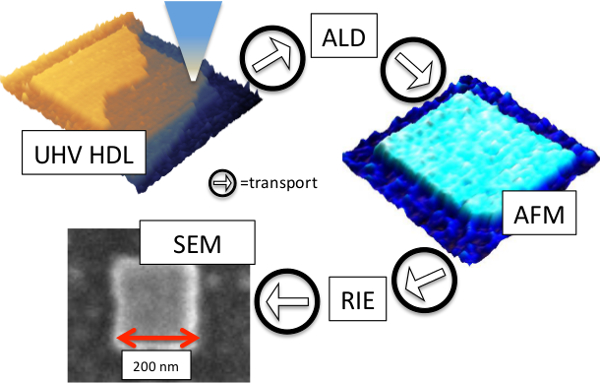
图1.原发性纳米制造工艺步骤。作为一个例子,一个200纳米×200平方纳米被示出。每个圆圈的箭头表示大气暴露和t的步骤站点之间ransport。特高压后,样品制备,样品是用特高压HDL其次是STM计量(左上)图案。 ALD然后进行,接着用AFM测量(右)。 RIE转成图案的Si(100),其次是SEM计量(左下)。 请点击此处查看该图的放大版本。

最精确的光刻迄今为止通常涉及扫描探针技术,具体地基于STM的图案化,其中原子分辨率的图案化和官能化已被证明对于许多应用7以前,原子操纵已生产纳米结构的最终精度通过使用单个原子作为构建块,8 ,9,10,但需要在低温条件,从而纳米结构缺乏长期稳定性。 RT原子操纵通过除去从表面的氢原子已被示出,specificalLY高密度脂蛋白。11,12,13的HDL有望使新的类的基础上,表面处理的对比空间定位电子和其他设备。使用的HDL,而不进一步处理,不同的器件架构是可能的,包括悬挂键合线或逻辑器件。14,15,16除了提供电相反,高密度脂蛋白可引入其中,所述钝化H膜层已被除去的表面上的化学对比,在效果创建用于进一步化学修饰的模板。这种化学修饰已被证明在硅和其它表面,显示出对金属,17绝缘体18,甚至半导体的沉积选择性。16,19这些例子都产生二维结构,因此其它处理步骤,必须使用以产生真正的三三维结构的原子分辨控制由高密度脂蛋白承诺。此前,这需要重复图案,19,20,21退火,22 </suP>或更少的很好的解决方法,如尖为基础的电子束诱导沉积。23

类似于电子束光刻,高密度脂蛋白使用电子的局部的磁通,以暴露抗蚀剂。有几个相似之处存在,如与临场变盘的大小和图案效率进行多模式光刻技术的能力。24然而,高密度脂蛋白的真正动力源于它是如何不同于电子束光刻。首先,抗蚀剂中的HDL是氢原子的单层以便抗蚀剂曝光成为数字过程;抗蚀原子或者是或不存在。25由于氢原子的位置对应于底层的Si(100)晶格HDL的过程可以是一个原子精确的过程,尽管应当注意的是,在本文所述的HDL具有纳米精度反对具有原子完美,因此不是数字在这种情况下。由于在高密度脂蛋白的电子源是本地到表面,STM操作的各种模式促进两者吞吐量的优化以及错误检查。在低于〜4.5 V针尖样的偏见,光刻可以在以原子精度,被称为以原子的精确模式(AP模式)的单个原子水平上进行。与此相反,在偏压以上〜7伏,电子直接从尖端到具有宽线宽并高去钝化效率,这里被称为场发射模式(FE模式)样品发出。 HDL吞吐量然后,可以通过仔细组合这两种模式进行优化,虽然整体的吞吐量保持小相对于电子束光刻用构图高达1微米2 /分钟的可能。当偏置被颠倒,使得样品保持在〜-2.25伏,电子隧道从样品到尖端极低激活操作效率,从而使该表面的原子结构的检查既用于纠错和原子级计量。

图1中所示的该纳米结构物的制造工艺</strong>的用UHV-HDL的步骤开始时,如上所述。以下的HDL,将样品排放到大气中,在该时间所述图案化的区域变得饱和与水,形成一个薄的( 即,〜1单层)SiO 226中传输后,将样品插入到一ALD室,用于沉积二氧化钛(TiO 2的),其厚度约2-3纳米这里沉积,如通过AFM和XPS 27由于二氧化钛反应取决于表面的水饱和度测量,该方法是可能的,尽管这浸透表面与水的气氛曝光。接着,在该ALD掩模图案转移到散装使用的RIE,使硅为20nm除去样品进行蚀刻,用原子力显微镜和SEM测定的蚀刻深度。为了便于计量步骤,在Si(100)晶片图案化有其目的是特高压制备由长工作距离的光学显微镜,原子力显微镜俯视光学成像后是可见的网格线,和低倍率俯视SEM图像。为了帮助识别纳米级结构,1微米2蛇形图案( 养老金计划 )进行构图到样品与位于相对于养老金计划固定位置最偏远的纳米图案。

高密度脂蛋白,选择性ALD,和RIE的这种组合可以是用于纳米结构制造的一个重要的过程,它包括在原子尺度计量作为该过程的一个天然副产品。下面,我们包括涉及制造亚10纳米的纳米结构中的Si(100),使用高密度脂蛋白,选择性ALD,和RIE步骤的详细描述。假定一个是本领域技术人员在这些方法中,但信息将包含有关如何对各种处理进行集成。特别强调将给予由作者,以防止同样的困难经历的那些意想不到的困难,特别是涉及到运输和计量。

Protocol

1. 前原位样品制备芯片的准备设计适当的蚀刻掩模将确定在硅(100)晶圆标记。使用标准的光刻和RIE,蚀刻线作为基准标记成从该STM样品将要采取的晶片的一个网格。该线应为10微米宽,1微米深,并在500微米的间距。蚀刻后,剥去样本剩余的光刻胶。 注意:基准标记必须是可识别的原位上的样品,以及在AFM及SEM计量期间尖端位置。 通过采用标准的粘性蓝色?…

Representative Results

在这里所描述的情况下,高密度脂蛋白是使用多模光刻进行。24在FE模式,具有8 V样品偏压,1 Na和0.2 MC /厘米(相当于50毫微米/秒尖端速度)进行,尖端移过的表面平行或垂直于硅晶格,产生激活操作的行。虽然这种线形很尖依赖,在这里的情况下,线的完全去钝化部分约为6纳米宽,具有部分去钝化延伸的线两侧另一个为2nm的尾巴。当高精细图案需要,可以使用4 V样值的偏差,4 nA的,和4 …

Discussion

上面所描述的纳米结构进行计量要求弥合期间使用其他工具如原子力显微镜和SEM HDL和图案位置的前端定位的能力。与此相反,以具有高分辨率位置编码其它发达构图工具,如电子束光刻,在这里进行的高密度脂蛋白,用一个STM进行而得到很好的控制粗定位,所以额外位置识别的协议被使用, 如图3首先,一个长焦距显微镜定位在超高真空系统从针尖 – 样品的结约20cm外。样品被构图为1…

Disclosures

The authors have nothing to disclose.

Acknowledgements

这项工作是由DARPA从(N66001-08-C-2040)合同,由得克萨斯州的新兴科技基金资助项目。作者要感谢智英金,格雷格Mordi,安吉拉Azcatl,汤姆沙尔夫对有关选择性原子层沉积的贡献,以及马丁·华莱士和戈登·波洛克易地来样加工。

Materials

Si Wafer VA Semiconductor P type (Boron) Si<100> +/- 2 degrees, 280 mm +/- 25 mm thick, 0.01-0.02 ohm-cm
Ta foil Alfa Aesar 335 0.025mm (0.001in) thick, 99.997% (metals basis)
Methanol Alfa Aesar 19393 Semiconductor Grade, 99.9%
2-Propanol Alfa Aesar 19397 Semiconductor Grade, 99.5%
Acetone Alfa Aesar 19392 Semiconductor Grade, 99.5%
Argon Praxair Ultra high purity (grade 5.0)
Deionized water Millipore Milli-Q Water Purification System >18 MW resistance water produced on demand.
TiCl4 Sigma Aldrigh 254312 ≥99.995% trace metals basis
O2 Matheson G2182101 Research Grade
SF6 Matheson G2658922 Ultra high purity (grade 4.7)
Blue Medium Tack Roll Semiconductor Equipment Corporation 18074 Thickness 75 um / .003”  Length 200 M / 660’ 

References

  1. Yoffe, A. D. Low-dimensional systems: quantum size effects and electronic properties of semiconductor microcrystallites (zero-dimensional systems) and some quasi-two-dimensional systems. Adv. in Phy. 42 (2), 173-262 (1993).
  2. Alivisatos, A. P. Semiconductor Clusters, Nanocrystals, and Quantum Dots. Science. 271 (5251), 933-937 (1996).
  3. Craighead, H. G. Nanoelectromechanical Systems. Science. 290 (5496), 1532-1535 (2000).
  4. Dai, M. D., Kim, C. -. W., Eom, K. Finite size effect on nanomechanical mass detection: the role of surface elasticity. Nanotechnology. 22 (26), 265502 (2011).
  5. Personick, M., Mirkin, C. Making sense of the mayhem behind shape control in the synthesis of gold nanoparticles. J. Am. Chem. Soc. 135 (C), 18238-18247 (2013).
  6. Rothemund, P. W. K., Ekani-Nkodo, A., et al. Design and Characterization of Programmable DNA. Nanotubes. J. Am. Chem. Soc. 26, 16344-16353 (2004).
  7. Hersam, M. C., Guisinger, N. P., Lyding, J. W. Silicon-based molecular nanotechnology. Nanotechnology. 11 (2), 70-76 (2000).
  8. Eigler, D. M., Schweizer, E. K. Positioning single atoms with a scanning tunnelling microscope. Nature. 344, 524-526 (1990).
  9. Heinrich, A. J., Lutz, C. P., Gupta, J. A., Eigler, D. M. Molecular cascades. Science. 298, 1381-1387 (2002).
  10. Crommie, M. F., Lutz, C. P., Eigler, D. M. Confinement of Electrons to Quantum Corrals on a Metal Surface. Science. 262 (5131), 218-220 (1993).
  11. Shen, T. -. C., Wang, C., et al. Atomic-Scale Desorption Through Electronic and Vibrational Excitation Mechanisms. Science. 268, 1590-1592 (1995).
  12. Randall, J. N., Lyding, J. W., et al. Atomic precision lithography on Si. J. Vac. Sci. Tech. B. 27 (6), 2764-2768 (2009).
  13. Tong, X., Wolkow, R. A. Electron-induced H atom desorption patterns created with a scanning tunneling microscope: Implications for controlled atomic-scale patterning on H-Si(100). Surf. Sci. 600 (16), L199-L203 (2006).
  14. Hitosugi, T., Hashizume, T., et al. Scanning Tunneling Spectroscopy of Dangling-Bond Wires Fabricated on the Si(100)-2×1-H Surface. Jap. J. App. Phys, Pt 2 2. 36 (3B), L361-L364 (1997).
  15. Bird, C. F., Fisher, A. J., Bowler, D. R. Soliton effects in dangling-bond wires on Si(001). Phys. Rev B. 68, 115318 (2003).
  16. Wolkow, R. A., Livadaru, L., et al. . Beyond-CMOS Electronics. , 1-28 (2013).
  17. Lyding, J. W., Shen, T. -. C., Hubacek, J. S., Tucker, J. R., Abeln, G. C. Nanoscale patterning and oxidation of H-passivated Si(100)-2×1 surfaces with an ultrahigh vacuum scanning tunneling microscope. App. Phys. Lett. 64 (15), 2010-2012 (1994).
  18. Lyding, J. W., Shen, T. -. C., Abeln, G. C., Wang, C., Tucker, J. R. Nanoscale patterning and selective chemistry of silicon surfaces by ultrahigh-vacuum scanning tunneling microscopy. Nanotechnology. 7, 128-133 (1996).
  19. Owen, J. H. G., Ballard, J., Randall, J. N., Alexander, J., Von Ehr, J. R. Patterned Atomic Layer Epitaxy of Si / Si(001):H. J. Vac. Sci. Tech. B. 29 (6), 06F201 (2011).
  20. Goh, K. E. J., Chen, S., Xu, H., Ballard, J., Randall, J. N., Ehr, J. R. Von Using patterned H-resist for controlled three-dimensional growth of nanostructures. App. Phys. Lett. 98 (16), 163102 (2011).
  21. Ye, W., Peña Martin, P. Direct writing of sub-5 nm hafnium diboride metallic nanostructures. ACS Nano. 4 (11), 6818-6824 (2010).
  22. Brien, J. L., Schofield, S. R., et al. Scanning tunnelling microscope fabrication of arrays of phosphorus atom qubits for a silicon quantum computer. Smart. 11 (5), 741-748 (2002).
  23. Van Oven, J. C., Berwald, F., Berggren, K. K., Kruit, P., Hagen, C. W. Electron-beam-induced deposition of 3-nm-half-pitch patterns on bulk Si. J. Vac. Sci. Tech. B. 29 (6), 06F305 (2011).
  24. Ballard, J. B., Sisson, T. W., et al. Multimode hydrogen depassivation lithography: A method for optimizing atomically precise write times. J. Vac. Sci. Tech. B. 31 (6), 06FC01 (2013).
  25. Randall, J. N., Ballard, J. B., et al. Atomic precision patterning on Si: An opportunity for a digitized process. Microelec. Eng. 87 (5-8), 955-958 (2010).
  26. Perrine, K. A., Teplyakov, A. V. Reactivity of selectively terminated single crystal silicon surfaces. Chem. Soc. Rev. 39 (8), 3256-3274 (2010).
  27. McDonnell, S., Longo, R. C., et al. Controlling the Atomic Layer Deposition of Titanium Dioxide on Silicon: Dependence on Surface Termination. The J. Phys. Chem. C. 117 (39), 20250-20259 (2013).
  28. Kane, D. F. Plasma cleaning of metal surfaces. J. Vac. Sci. Tech. 11 (3), 567 (1974).
  29. Hersam, M. C., Guisinger, N. P., Lyding, J. W., Thompson, D. S., Moore, J. S. Atomic-level study of the robustness of the Si(100)-2×1:H surface following exposure to ambient conditions. App. Phys. Lett. 78 (7), 886-888 (2001).
  30. Agostino, R., Flamm, D. L. Plasma etching of Si and SiO2 in SF6–O2 mixtures. J. App. Phys. 52 (1), 162 (1981).
  31. Longo, R. C., McDonnell, S., et al. Selectivity of metal oxide atomic layer deposition on hydrogen terminated and oxidized Si(001)-(2×1) surface. J. Vac. Sci Tech. B. 32 (3), 03D112 (2014).
  32. Ruess, F. J., Oberbeck, L., et al. The use of etched registration markers to make four-terminal electrical contacts to STM-patterned nanostructures. Nanotechnology. 16 (10), 2446-2449 (2005).
  33. Ruess, F. J., Pok, W., et al. Realization of Atomically Controlled Dopant Devices in Silicon. Small. 3 (4), 563-567 (2007).
  34. Li, K., Namboodiri, P., et al. Controlled formation of atomic step morphology on micropatterned Si (100). J. Vac. Sci. Tech. B. 29 (4), 041806 (2011).
  35. Ballard, J. B., Owen, J. H. G., et al. Pattern transfer of hydrogen depassivation lithography patterns into silicon with atomically traceable placement and size control. Journal of Vacuum Science and Technology B. 32 (4), 041804 (2014).
  36. Gusev, E. P., Cabral, C., Copel, M., D’Emic, C., Gribelyuk, M. U ltrathin HfO 2 films grown on silicon by atomic layer deposition for advanced gate dielectrics applications. Microelectronic Engineering. 69, 145-151 (2003).
check_url/52900?article_type=t

Play Video

Cite This Article
Ballard, J. B., Dick, D. D., McDonnell, S. J., Bischof, M., Fu, J., Owen, J. H. G., Owen, W. R., Alexander, J. D., Jaeger, D. L., Namboodiri, P., Fuchs, E., Chabal, Y. J., Wallace, R. M., Reidy, R., Silver, R. M., Randall, J. N., Von Ehr, J. Atomically Traceable Nanostructure Fabrication. J. Vis. Exp. (101), e52900, doi:10.3791/52900 (2015).

View Video